|
поискавой системы для электроныых деталей |
|
|
поискавой системы для электроныых деталей |
|
ADP1053ACPZ-R7 датащи(PDF) 25 Page - Analog Devices |
|
|
|||||||||||||||||||||||||||||
ADP1053ACPZ-R7 датащи(HTML) 25 Page - Analog Devices |
|
|
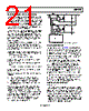
25 / 84 page  Data Sheet ADP1053 Rev. A | Page 25 of 84 POWER MONITORING AND FLAGS The ADP1053 has extensive system and fault monitoring capabilities for the sensed signals. The system monitoring functions include voltage, current, power, and temperature readings. The fault conditions include out-of-limit values for current, voltage, power, and temperature. The limits for the fault conditions are programmable. The ADP1053 has an extensive set of flags that are set when certain thresholds or limits are reached. For information about the thresholds and limits, see the Flag Registers section. MONITORING FUNCTIONS The ADP1053 monitors and reports several signals, including voltages, currents, power, and temperature. All these values are stored in individual registers and can be read through the PMBus/I2C interface. The accuracy of the ADP1053 is specified relative to the full- scale range (FSR) of the signal that is measured. VOLTAGE READINGS VS_A and VS_B Readings The VS_A and VS_B voltage value registers (Register 0xFED5 and Register 0xFED6, respectively) are updated every 10 ms. The VS_A and VS_B ADCs have an input range of 0 V to 1.6 V and a resolution of 12 bits, which means that the LSB size is 1.6 V/4096 = 390.6 μV. The valid input range is 1.5 V, which means that the maximum ADC output code is limited to 1.5 V/390.6 μV = 3840. The equation to calculate the ADC code at a specified voltage (VX) is given by the following formula: ADC CODE = VX/390.6 μV For example, when there is 1 V on the input of the VS_A ADC, VS_A ADC CODE = 1 V/390.6 μV = 2560 ACSNS Readings The ACSNS voltage value register (Register 0xFED9) is updated every 1 ms. The ACSNS ADC has an input range of 0 V to 1.6 V and a resolution of 11 bits, which means that the LSB size is 1.6 V/ 2048 = 781.25 μV. The valid input range is 1.4 V, which means that the ADC output code is limited to 1.4 V/781.25 μV = 1792. The equation to calculate the ADC code at a specified voltage (VX) is given by the following formula: ADC CODE = VX/781.25 μV For example, when there is 1 V on the input of the ACSNS ADC, ACSNS ADC CODE = 1 V/781.25 μV = 1280 CURRENT READINGS By default, the current reading ADCs are updated every 10 ms. However, Register 0xFE89 can be used to change the update rate to 50 ms, 100 ms, or 200 ms. CS and CS1 (CS1_A/CS1_B) Readings The CS, CS1_A, and CS1_B value registers (Register 0xFED0, Register 0xFED1, and Register 0xFED2, respectively) are updated every 10 ms. The CS, CS1_A, and CS1_B ADCs have an input range of 0 V to 1.6 V and a resolution of 12 bits, which means that the LSB size is 1.6 V/4096 = 390.6 μV. The equation to calculate the ADC code at a specified voltage (VX) is given by the following formula: ADC CODE = VX/390.6 μV For example, when there is 1 V on the input of the CS ADC, CS ADC CODE = 1 V/390.6 μV = 2560 CS2 (CS2_A/CS2_B) Readings The CS2_A and CS2_B value registers (Register 0xFED3 and Register 0xFED4, respectively) are updated every 10 ms. The CS2_A and CS2_B ADCs have an input range of 0 mV to 120 mV and a resolution of 12 bits, which means that the LSB size is 120 mV/4096 = 29.3 μV. The equation to calculate the ADC code at a specified voltage (VX) is given by the following formula: ADC CODE = VX × 4096/Sensing Range For example, when there is 40 mV on the input of the CS2_A ADC and the sensing range is 120 mV, CS2_A ADC CODE = 40 mV × 4096/120 mV = 1365 TEMPERATURE READINGS (RTD1 AND RTD2 PINS) The RTD1 and RTD2 pins are provided for use with an external 100 kΩ NTC thermistor. An internal current source of 10 μA, 20 μA, 30 μA, or 40 μA can be selected. Therefore, with a 100 kΩ thermistor, the voltage on the RTDx pin is 1 V at 25°C. An ADC on the ADP1053 monitors the voltage on each RTDx pin. The ADC has a 1 kHz bandwidth and 12-bit resolution. The ADC reading is used for overtemperature protection and monitoring. For more information, see the Overtemperature Protection (OTP) and Overtemperature Warning (OTW) Flags section and the Temperature Linearization Scheme section. ADP1053 ADC ADC OTP1 OTP2 THRESHOLD THRESHOLD RTD TEMPERATURE REGISTERS NTC 100kΩ NTC 100kΩ RTD1 RTD2 Figure 23. RTD Pin Internal Details |
|
ссылки URL |
| Вашему бизинису помогли Аллдатащит? [ DONATE ] |
Что такое Аллдатащит | реклама | контакт | Конфиденциальность | Ссылка на техническое описание | обмен ссыками | поиск по производителю All Rights Reserved©Alldatasheet.com |
| Russian : Alldatasheetru.com | Korean : Alldatasheet.co.kr | Spanish : Alldatasheet.es | French : Alldatasheet.fr | Italian : Alldatasheetit.com Portuguese : Alldatasheetpt.com | Polish : Alldatasheet.pl | Vietnamese : Alldatasheet.vn Indian : Alldatasheet.in | Mexican : Alldatasheet.com.mx | British : Alldatasheet.co.uk | New Zealand : Alldatasheet.co.nz |
|
Family Site : ic2ic.com |
icmetro.com |
 Russian ▼
 English
 Chinese
 German
 Japanese
 Russian
 Korean
 Spanish
 French
 Italian
 Portuguese
 Polish
 Vietnamese
 Indian
 Mexican
 British
 New Zealand