|
поискавой системы для электроныых деталей |
|
|
поискавой системы для электроныых деталей |
|
ADP1053ACPZ-R7 датащи(PDF) 15 Page - Analog Devices |
|
|
|||||||||||||||||||||||||||||
ADP1053ACPZ-R7 датащи(HTML) 15 Page - Analog Devices |
|
|
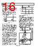
15 / 84 page  Data Sheet ADP1053 Rev. A | Page 15 of 84 Example Configuration of PWM Outputs Table 6 provides example register settings that configure the OUT1 and OUT2 outputs for Channel A. In this example, the switching frequency of Channel A is 208.3 kHz, that is, a 4.8 μs switching cycle (Register 0xFE0A = 0x15). GO Command All eight PWM outputs work together. Therefore, when repro- gramming more than one of these outputs, it is important to first update all the registers and then latch the information into the ADP1053 at the same time using the GO command (Bit 2 of Register 0xFE61). During reprogramming, the outputs are temporarily disabled. A special instruction is sent to the ADP1053 to ensure that new timing information is programmed simulta- neously. It is recommended that unused PWM outputs be disabled. Modulation Settings Bits[3:0] in each PWM output setting register enable/disable rising and falling edge modulation and set the modulation sign. When the modulation sign is positive, an increase of the feedback filter output moves the edge to the right. When the sign is nega- tive, an increase of the filter output moves the edge to the left. For example, one of the most widely used modulation schemes is trailing edge modulation. To realize this scheme, Bits[3:0] of the PWM output setting registers are set to 0010. Modulation Limits Register 0xFE3C and Register 0xFE3D can be programmed to apply a maximum duty cycle modulation limit to PWM signals in Channel A and Channel B, respectively. As shown in Figure 8, this limit is the maximum time variation for the modulated edges from the default timing, following the configured modulation direction. There is no minimum duty cycle limit setting. There- fore, the user must set the rising edges and falling edges based on the case with the least modulation. tRX tFX tRY tFY t0 tS/2 tS 3 tS/2 OUTX OUTY tMOD_LIMIT tMOD_LIMIT Figure 8. Setting Modulation Limits The step size of an LSB in Register 0xFE3C and Register 0xFE3D depends on the switching frequency (see Table 5). Table 5. LSB Step Size and Switching Frequency Switching Frequency LSB Step Size 48.8 kHz to 86.8 kHz 80 ns 97.7 kHz to 183.8 kHz 40 ns 195.3 kHz to 378.8 kHz 20 ns 390.6 kHz to 625.0 kHz 10 ns The modulated edges cannot exceed one switching cycle. For PWM outputs without the 180° phase shift, such as OUTX in Figure 7, the edges before and after modulation are always from t0 to tS. For PWM outputs with the 180° phase shift, such as OUTY in Figure 7, the edges before and after modulation are always from tS/2 to 3tS/2. The GUI provided with the ADP1053 is recommended for evaluating this feature. Table 6. Example OUT1 and OUT2 Configuration Register Setting Configuration Register 0xFE43, Bits[6:5] = 00 The PWM output OUT1 is assigned to Channel A with a frequency of 208.3 kHz. Register 0xFE43, Bit 7 = 0 The reference for the rising and falling edges of OUT1 is the start of the switching cycle (180° phase shift disabled). Register 0xFE40 = 0x01 and Register 0xFE42 = 0x00 The rising edge value is 0x010 (16 decimal), and the timing is set to 16 × 5 ns = 80 ns. Register 0xFE41 = 0x20 The falling edge value is 0x200 (512 decimal), and the timing is set to 512 × 5 ns = 2.56 μs. Register 0xFE47, Bits[6:5] = 00 The PWM output OUT2 is also assigned to Channel A with a frequency of 208.3 kHz. Register 0xFE47, Bit 7 = 1 The reference for the rising and falling edges of OUT2 is half the switching cycle, tS/2 (180° phase shift enabled). Register 0xFE44 = 0x01 and Register 0xFE46 = 0x00 The rising edge value is 0x010 (16 decimal). Due to the 180° phase shift, the timing is set to 16 × 5 ns + 2.4 μs = 2.48 μs. Register 0xFE45 = 0x20 The falling edge value is 0x200 (512 decimal), and the timing is set to 512 × 5 ns + 2.48 μs = 5.04 μs. |
|
ссылки URL |
| Вашему бизинису помогли Аллдатащит? [ DONATE ] |
Что такое Аллдатащит | реклама | контакт | Конфиденциальность | Ссылка на техническое описание | обмен ссыками | поиск по производителю All Rights Reserved©Alldatasheet.com |
| Russian : Alldatasheetru.com | Korean : Alldatasheet.co.kr | Spanish : Alldatasheet.es | French : Alldatasheet.fr | Italian : Alldatasheetit.com Portuguese : Alldatasheetpt.com | Polish : Alldatasheet.pl | Vietnamese : Alldatasheet.vn Indian : Alldatasheet.in | Mexican : Alldatasheet.com.mx | British : Alldatasheet.co.uk | New Zealand : Alldatasheet.co.nz |
|
Family Site : ic2ic.com |
icmetro.com |
 Russian ▼
 English
 Chinese
 German
 Japanese
 Russian
 Korean
 Spanish
 French
 Italian
 Portuguese
 Polish
 Vietnamese
 Indian
 Mexican
 British
 New Zealand