|
поискавой системы для электроныых деталей |
|
|
поискавой системы для электроныых деталей |
|
ADP1053ACPZ-R7 датащи(PDF) 16 Page - Analog Devices |
|
|
|||||||||||||||||||||||||||||
ADP1053ACPZ-R7 датащи(HTML) 16 Page - Analog Devices |
|
|
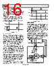
16 / 84 page  ADP1053 Data Sheet Rev. A | Page 16 of 84 FREQUENCY SYNCHRONIZATION Synchronization Output The FLGO/SYNO pin can be programmed to generate a synchro- nization reference output using Bit 3 of Register 0xFE0F. The pin outputs a 320 ns pulse-width signal, whose frequency follows either Channel A or Channel C (programmable using Bit 3 of Register 0xFE0E). To compensate for the propagation delays in the ADP1053 synchronization scheme, the SYNO signal has a 760 ns lead time before the start of the switching cycle. Figure 9 shows an example of the SYNO timing when using Channel A as the reference. 760ns t0 tS CLOCKA SYNO 320ns Figure 9. SYNO Timing Synchronization Input When the FLGI/SYNI pin is configured as a synchronization input, the external clock frequency at the pin must be between 90% and 110% of the internal switching frequency set by the channel’s internal switching frequency register. If the switching cycle is out of this range or if there is no rising edge detected for 80 μs, the part exits synchronization mode, and each channel operates at its preset internal switching frequency. The maximum external synchronization clock frequency should be less than 625 kHz. If the FLGI/SYNI pin is programmed for the FLGI function, the synchronization function is disabled. If two or more channels are enabled for synchronization, the valid synchronization frequency range is determined by the channel with the lowest synchronization multiple. The multiple is set using Bits[7:6] of Register 0xFE0A (Channel A), Register 0xFE0B (Channel B), and Register 0xFE0C (Channel C). If the multiple value is the same for two or more channels, the value set for Channel A has the highest priority and the value set for Channel C has the lowest priority. Note that if Channel A or Channel C is synchronized with an external clock at the SYNI pin, the SYNO frequency is the preset internal frequency but not the operating switching frequency. For example, if the preset frequency of Channel A is 100 kHz and the SYNO frequency is configured to follow Channel A, the SYNO frequency is still 100 kHz even when the external synchronization clock is at 105 kHz. To ensure proper operation of the synchronization mode, the synchronization multiple for at least one channel must be set to 1 (Bits[7:6] = 00). 760ns + tSYNC_DELAY t0 tS/2 tS CLOCKA CLOCKC CLOCKSYNC SYNI Figure 10. Synchronization Timing VOLTAGE SENSE Multiple voltage sense inputs on the ADP1053 are used for the monitoring, control, and protection of the power supply output. The voltage information is available through the PMBus/I2C interface. All voltage sense points can be calibrated digitally to remove any errors due to external components. This calibration can be performed in the production environment, and the settings saved in the EEPROM of the ADP1053. For more information, see the Power Supply Calibration and Trim section. The update rate of the ADC from a control loop standpoint is set to the switching frequency. For example, if the switching frequency is set to 100 kHz, the ADC outputs a signal at a rate of 100 kHz to the control loop. Because the Σ-Δ ADC samples at 1.6 MHz, the output of the ADC is the average of the 16 readings per switching cycle. ADP1053 HIGH SPEED ADC2 ACCURATE ADC1 LOAD DAC 6 BITS OVP DIGITAL FILTER VOLTAGE SENSE REGISTERS VS+_A/ VS+_B VS–_A/ VS–_B UVP THRESHOLD PGND_A/ PGND_B OVP_A/ OVP_B R3 R4 R1 R2 Figure 11. Voltage Sense Configuration |
|
ссылки URL |
| Вашему бизинису помогли Аллдатащит? [ DONATE ] |
Что такое Аллдатащит | реклама | контакт | Конфиденциальность | Ссылка на техническое описание | обмен ссыками | поиск по производителю All Rights Reserved©Alldatasheet.com |
| Russian : Alldatasheetru.com | Korean : Alldatasheet.co.kr | Spanish : Alldatasheet.es | French : Alldatasheet.fr | Italian : Alldatasheetit.com Portuguese : Alldatasheetpt.com | Polish : Alldatasheet.pl | Vietnamese : Alldatasheet.vn Indian : Alldatasheet.in | Mexican : Alldatasheet.com.mx | British : Alldatasheet.co.uk | New Zealand : Alldatasheet.co.nz |
|
Family Site : ic2ic.com |
icmetro.com |
 Russian ▼
 English
 Chinese
 German
 Japanese
 Russian
 Korean
 Spanish
 French
 Italian
 Portuguese
 Polish
 Vietnamese
 Indian
 Mexican
 British
 New Zealand