|
поискавой системы для электроныых деталей |
|
|
поискавой системы для электроныых деталей |
|
ADP1053ACPZ-R7 датащи(PDF) 55 Page - Analog Devices |
|
|
|||||||||||||||||||||||||||||
ADP1053ACPZ-R7 датащи(HTML) 55 Page - Analog Devices |
|
|
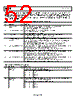
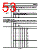
55 / 84 page  Data Sheet ADP1053 Rev. A | Page 55 of 84 When synchronization is enabled, the controller takes the SYNI signal, adds the tSYNC_DELAY, together with the 760 ns propagation delay, to generate the internal synchronization reference clock, as shown in Figure 40. Each channel then uses the reference clock (or a multiple of the reference clock if programmed in Register 0xFE0A, Register 0xFE0B, or Register 0xFE0C) to generate its own clock. Register 0xFE0D is used to set the tSYNC_DELAY time. 760ns + tSYNC_DELAY t0 tS CLOCKSYNC SYNI Figure 40. Synchronization Timing Table 37. Register 0xFE0D—Frequency Synchronization Delay Time Bits Bit Name R/W Description [7:0] tSYNC_DELAY R/W This register sets the additional delay of the synchronization reference clock to the rising edge of the SYNI pin signal. Each LSB corresponds to 80 ns resolution. Table 38. Register 0xFE0E—SYNO Selection and Synchronization Enable Bits Bit Name R/W Description [7:4] Reserved R/W Reserved. 3 SYNO selection R/W 0 = select Channel C as the SYNO reference. 1 = select Channel A as the SYNO reference. 2 Enable Channel C synchronization R/W Setting this bit enables frequency synchronization for Channel C. 1 Enable Channel B synchronization R/W Setting this bit enables frequency synchronization for Channel B. 0 Enable Channel A synchronization R/W Setting this bit enables frequency synchronization for Channel A. Table 39. Register 0xFE0F—Flag/Synchronization Pin Functions Bits Bit Name R/W Description 7 Reserved R/W Reserved. 6 Channel B filter 180° interleaving R/W Setting this bit enables 180° interleaving on the clock for the ADC and filter of Channel B. This setting prevents additional delays when the PWM outputs in Channel B use 180° interleaving. 5 FLAGOUT polarity R/W Setting this bit inverts the polarity of the FLGO/SYNO pin signal when the pin is programmed as a flag output (FLAGOUT). 0 = normal mode. A high signal on the FLGO/SYNO pin sets FLAGOUT. 1 = inverted. A low signal on the FLGO/SYNO pin sets FLAGOUT. 4 FLAGOUT selection R/W This bit configures the FLGO/SYNO pin to respond to the LIGHTLOAD_A or LIGHTLOAD_B flag. 0 = LIGHTLOAD_A flag triggers FLAGOUT. 1 = LIGHTLOAD_B flag triggers FLAGOUT. 3 FLGO/SYNO pin function selection R/W This bit configures the FLGO/SYNO pin as a flag output or a synchronization output. 0 = FLGO/SYNO pin used as a synchronization output (SYNO). 1 = FLGO/SYNO pin used as a flag output (FLAGOUT). 2 FLAGIN polarity R/W Setting this bit inverts the polarity of the FLGI/SYNI pin signal when the pin is programmed as a flag input (FLAGIN). 0 = normal mode. A high signal on the FLGI/SYNI pin sets FLAGIN. 1 = inverted. A low signal on the FLGI/SYNI pin sets FLAGIN. 1 FLAGIN debounce time R/W This bit sets the debounce time for FLAGIN. 0 = 0 μs debounce time for FLAGIN. 1 = 100 μs debounce time for FLAGIN. 0 FLGI/SYNI pin function selection R/W This bit configures the FLGI/SYNI pin as a flag input or a synchronization input. 0 = FLGI/SYNI pin used as a synchronization input (SYNI). 1 = FLGI/SYNI pin used as a flag input (FLAGIN). |
|
ссылки URL |
| Вашему бизинису помогли Аллдатащит? [ DONATE ] |
Что такое Аллдатащит | реклама | контакт | Конфиденциальность | Ссылка на техническое описание | обмен ссыками | поиск по производителю All Rights Reserved©Alldatasheet.com |
| Russian : Alldatasheetru.com | Korean : Alldatasheet.co.kr | Spanish : Alldatasheet.es | French : Alldatasheet.fr | Italian : Alldatasheetit.com Portuguese : Alldatasheetpt.com | Polish : Alldatasheet.pl | Vietnamese : Alldatasheet.vn Indian : Alldatasheet.in | Mexican : Alldatasheet.com.mx | British : Alldatasheet.co.uk | New Zealand : Alldatasheet.co.nz |
|
Family Site : ic2ic.com |
icmetro.com |
 Russian ▼
 English
 Chinese
 German
 Japanese
 Russian
 Korean
 Spanish
 French
 Italian
 Portuguese
 Polish
 Vietnamese
 Indian
 Mexican
 British
 New Zealand