|
поискавой системы для электроныых деталей |
|
|
поискавой системы для электроныых деталей |
|
ADP1053ACPZ-R7 датащи(PDF) 79 Page - Analog Devices |
|
|
|||||||||||||||||||||||||||||
ADP1053ACPZ-R7 датащи(HTML) 79 Page - Analog Devices |
|
|
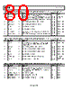
79 / 84 page  Data Sheet ADP1053 Rev. A | Page 79 of 84 Table 129. Register 0xFE8A—OTW1/OTW2 Settings Bits Bit Name R/W Description 7 OTW2 flag debounce R/W This bit sets the OTW2 flag debounce time. 0 = 100 ms. 1 = 0 ms. 6 OTW2 triggers PGOOD_B R/W This bit specifies whether the OTW2 flag triggers PGOOD_B. 0 = OTW2 does not trigger PGOOD_B. 1 = OTW2 triggers PGOOD_B. These bits set the OTW2 threshold. Bit 5 Bit 4 OTW2 Threshold 0 0 3.125 mV (1 LSB) above the OTP2 threshold 0 1 6.25 mV (2 LSBs) above the OTP2 threshold 1 0 9.375 mV (3 LSBs) above the OTP2 threshold [5:4] OTW2 threshold R/W 1 1 12.5 mV (4 LSBs) above the OTP2 threshold 3 OTW1 flag debounce R/W This bit sets the OTW1 flag debounce time. 0 = 100 ms. 1 = 0 ms. 2 OTW1 triggers PGOOD_A R/W This bit specifies whether the OTW1 flag triggers PGOOD_A. 0 = OTW1 does not trigger PGOOD_A. 1 = OTW1 triggers PGOOD_A. These bits set the OTW1 threshold. Bit 1 Bit 0 OTW1 Threshold 0 0 3.125 mV (1 LSB) above the OTP1 threshold 0 1 6.25 mV (2 LSBs) above the OTP1 threshold 1 0 9.375 mV (3 LSBs) above the OTP1 threshold [1:0] OTW1 threshold R/W 1 1 12.5 mV (4 LSBs) above the OTP1 threshold FLAG REGISTERS Register 0xFEC0 through Register 0xFEC4 are flag registers that indicate the status of the flags. Register 0xFEC5 through Register 0xFEC9 are latched flag registers. In the latched flag registers, flags are not reset when the condition disappears but remain set so that intermittent faults can be detected. Flags in the latched flag registers are cleared only by a register read (provided that the fault no longer exists) or by asserting PSON. It is recommended that the latched flag register be read again after the faults disappear to ensure that the register was reset. Note that latched flag bits are clocked on a low-to-high transition only. Table 130. Register 0xFEC0—Flag Register 1 and Register 0xFEC5—Latched Flag Register 1 (1 = Fault, 0 = Normal Operation) Bits Bit Name R/W Description Register Action 7 POWER_SUPPLY_A R Channel A power supply is off and the PWM outputs are disabled. This bit stays high until PSON_A is asserted. None 6 PGOOD_A R Power-good fault on Channel A. This flag is set when the UVP_A, POWER_SUPPLY_A, EEPROM_CRC, or SOFTSTART_FILTER_A flag is set. The ACSNS and OTW1 flags can also be programmed to be included. 0xFE09, 0xFE78, 0xFE8A PGOOD_A pin set low 5 CS1_A_OCP R The voltage at CS1_A is above the 1.2 V threshold. 0xFE00, 0xFE70 Programmable 4 CS2_A_OCP R The voltage at CS2_A is above its threshold. 0xFE01, 0xFE18 Programmable 3 UVP_A R VS_A is below its threshold. 0xFE03, 0xFE28 Programmable 2 OVP_A R OVP_A is above its threshold. 0xFE02, 0xFE26 Programmable 1 LIGHTLOAD_A R Channel A is in light load mode (CS2_A current is below the light load threshold). 0xFE1A, 0xFE69 Programmable 0 VS_SET_ERR_A R The intended VS_A reference setting is outside the allowed range. 0xFE1E, 0xFE20 None |
|
ссылки URL |
| Вашему бизинису помогли Аллдатащит? [ DONATE ] |
Что такое Аллдатащит | реклама | контакт | Конфиденциальность | Ссылка на техническое описание | обмен ссыками | поиск по производителю All Rights Reserved©Alldatasheet.com |
| Russian : Alldatasheetru.com | Korean : Alldatasheet.co.kr | Spanish : Alldatasheet.es | French : Alldatasheet.fr | Italian : Alldatasheetit.com Portuguese : Alldatasheetpt.com | Polish : Alldatasheet.pl | Vietnamese : Alldatasheet.vn Indian : Alldatasheet.in | Mexican : Alldatasheet.com.mx | British : Alldatasheet.co.uk | New Zealand : Alldatasheet.co.nz |
|
Family Site : ic2ic.com |
icmetro.com |
 Russian ▼
 English
 Chinese
 German
 Japanese
 Russian
 Korean
 Spanish
 French
 Italian
 Portuguese
 Polish
 Vietnamese
 Indian
 Mexican
 British
 New Zealand