|
поискавой системы для электроныых деталей |
|
|
поискавой системы для электроныых деталей |
|
ADP1053ACPZ-R7 датащи(PDF) 67 Page - Analog Devices |
|
|
|||||||||||||||||||||||||||||
ADP1053ACPZ-R7 датащи(HTML) 67 Page - Analog Devices |
|
|
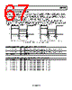
67 / 84 page  Data Sheet ADP1053 Rev. A | Page 67 of 84 SYNCHRONIZATION SETTING REGISTERS If the synchronization cycle for Channel A, Channel B, or Channel C is tS, and tS is programmed to be synchronized to the switching cycle, tSYNC, the on times of the PWM outputs in this channel remain the same. For example, if OUTX and OUTY are assigned to Channel C and OUTY is programmed for a 180°C phase shift, the difference between the falling edge of OUTX and the rising edge of OUTY changes to tSYNC/2 − tFX, as shown on the left side of Figure 44. If the timing of the outputs is critical—for example, when OUTX and OUTY drive two switches in a totem-pole structure—the operation of the power stage may be significantly affected. Register 0xFE66 enables PWM output edge adjustment for OUT1 to OUT8. When the appropriate bit is set in Register 0xFE66, an adjustment of (tS − tSYNC)/2 is made on both edges of the corresponding PWM output. It is important to enable output adjustment for the complementary OUTX/ OUTY pairs. With output edge adjustment set on both OUTX and OUTY (as shown on the right side of Figure 44), the dead time between the falling edge of OUTX and the rising edge of OUTY is kept the same at tS/2 − tFX. tFX tFX – (tS – tSYNC)/2 tFY tFY – (tS – tSYNC)/2 tSYNC/2 tSYNC/2 tSYNC tSYNC t0 t0 OUTX OUTY OUTX OUTY tSYNC/2 – tFX tS/2 – tFX tS/2 – tFY tSYNC/2 – tFY SYNCHRONIZATION WITH NO EDGE ADJUSTMENT ON tFX AND tFY SYNCHRONIZATION WITH EDGE ADJUSTMENT ON tFX AND tFY Figure 44. PWM Output Edge Adjustment in Channel C Synchronization Table 95. Register 0xFE65—OUT1 and OUT2 Shutdown in Channel C Synchronization Bits Bit Name R/W Description 7 OUT2 shutdown R/W Setting this bit shuts down OUT2 at the start of the OUT1 switching cycle. If OUT2 is not assigned to Channel C, this bit must be set to 0. 6 OUT1 shutdown R/W Setting this bit shuts down OUT1 at the start of the OUT2 switching cycle. If OUT1 is not assigned to Channel C, this bit must be set to 0. [5:0] Reserved R/W Reserved. Table 96. Register 0xFE66—OUT1 Through OUT8 Dead Time Adjustment in Synchronization Bits Bit Name R/W Description 7 OUT8 adjustment R/W Setting this bit adjusts both edges of OUT8 by (tS − tSYNC)/2. 6 OUT7 adjustment R/W Setting this bit adjusts both edges of OUT7 by (tS − tSYNC)/2. 5 OUT6 adjustment R/W Setting this bit adjusts both edges of OUT6 by (tS − tSYNC)/2. 4 OUT5 adjustment R/W Setting this bit adjusts both edges of OUT5 by (tS − tSYNC)/2. 3 OUT4 adjustment R/W Setting this bit adjusts both edges of OUT4 by (tS − tSYNC)/2. 2 OUT3 adjustment R/W Setting this bit adjusts both edges of OUT3 by (tS − tSYNC)/2. 1 OUT2 adjustment R/W Setting this bit adjusts both edges of OUT2 by (tS − tSYNC)/2. 0 OUT1 adjustment R/W Setting this bit adjusts both edges of OUT1 by (tS − tSYNC)/2. |
|
ссылки URL |
| Вашему бизинису помогли Аллдатащит? [ DONATE ] |
Что такое Аллдатащит | реклама | контакт | Конфиденциальность | Ссылка на техническое описание | обмен ссыками | поиск по производителю All Rights Reserved©Alldatasheet.com |
| Russian : Alldatasheetru.com | Korean : Alldatasheet.co.kr | Spanish : Alldatasheet.es | French : Alldatasheet.fr | Italian : Alldatasheetit.com Portuguese : Alldatasheetpt.com | Polish : Alldatasheet.pl | Vietnamese : Alldatasheet.vn Indian : Alldatasheet.in | Mexican : Alldatasheet.com.mx | British : Alldatasheet.co.uk | New Zealand : Alldatasheet.co.nz |
|
Family Site : ic2ic.com |
icmetro.com |
 Russian ▼
 English
 Chinese
 German
 Japanese
 Russian
 Korean
 Spanish
 French
 Italian
 Portuguese
 Polish
 Vietnamese
 Indian
 Mexican
 British
 New Zealand