|
поискавой системы для электроныых деталей |
|
|
поискавой системы для электроныых деталей |
|
ADP1053ACPZ-R7 датащи(PDF) 64 Page - Analog Devices |
|
|
|||||||||||||||||||||||||||||
ADP1053ACPZ-R7 датащи(HTML) 64 Page - Analog Devices |
|
|
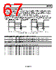
64 / 84 page  ADP1053 Data Sheet Rev. A | Page 64 of 84 PWM OUTPUT TIMING REGISTERS Figure 43 shows the timing of the rising and falling edges of the PWM outputs. Register 0xFE40 to Register 0xFE5F describe the implementation and programming of the eight PWM signals that are output from the ADP1053. In Figure 43, OUTX is an example of PWM timing without the 180° phase shift setting, and OUTY is an example of PWM timing with the 180° phase shift setting. tRX tFX tRY tFY t0, START OF SWITCHING CYCLE tS, END OF SWITCHING CYCLE tS/2 3 tS/2 OUTX OUTY Figure 43. PWM Output Timing Diagram Table 86. Register 0xFE40/0xFE44/0xFE48/0xFE4C/0xFE50/0xFE54/0xFE58/0xFE5C—OUT1 to OUT8 Rising Edge Timing (MSBs) Bits Bit Name R/W Description [7:0] OUTX rising edge timing (tRX), MSBs R/W This register contains the eight MSBs of the 12-bit tRX time. This value is always used with Bits[7:4] of Register 0xFE42/0xFE46/0xFE4A/0xFE4E/0xFE52/0xFE56/0xFE5A/0xFE5E, which contains the four LSBs of the tRX time. Each LSB corresponds to 5 ns resolution. Table 87. Register 0xFE41/0xFE45/0xFE49/0xFE4D/0xFE51/0xFE55/0xFE59/0xFE5D—OUT1 to OUT8 Falling Edge Timing (MSBs) Bits Bit Name R/W Description [7:0] OUTX falling edge timing (tFX), MSBs R/W This register contains the eight MSBs of the 12-bit tFX time. This value is always used with Bits[3:0] of Register 0xFE42/0xFE46/0xFE4A/0xFE4E/0xFE52/0xFE56/0xFE5A/0xFE5E, which contains the four LSBs of the tFX time. Each LSB corresponds to 5 ns resolution. Table 88. Register 0xFE42/0xFE46/0xFE4A/0xFE4E/0xFE52/0xFE56/0xFE5A/0xFE5E—OUT1 to OUT8 Rising and Falling Edge Timing (LSBs) Bits Bit Name R/W Description [7:4] OUTX rising edge timing (tRX), LSBs R/W These bits contain the four LSBs of the 12-bit tRX time. This value is always used with the eight bits of Register 0xFE40/0xFE44/0xFE48/0xFE4C/0xFE50/0xFE54/0xFE58/0xFE5C, which contains the eight MSBs of the tRX time. Each LSB corresponds to 5 ns resolution. [3:0] OUTX falling edge timing (tFX), LSBs R/W These bits contain the four LSBs of the 12-bit tFX time. This value is always used with the eight bits of Register 0xFE41/0xFE45/0xFE49/0xFE4D/0xFE51/0xFE55/0xFE59/0xFE5D, which contains the eight MSBs of the tFX time. Each LSB corresponds to 5 ns resolution. |
|
ссылки URL |
| Вашему бизинису помогли Аллдатащит? [ DONATE ] |
Что такое Аллдатащит | реклама | контакт | Конфиденциальность | Ссылка на техническое описание | обмен ссыками | поиск по производителю All Rights Reserved©Alldatasheet.com |
| Russian : Alldatasheetru.com | Korean : Alldatasheet.co.kr | Spanish : Alldatasheet.es | French : Alldatasheet.fr | Italian : Alldatasheetit.com Portuguese : Alldatasheetpt.com | Polish : Alldatasheet.pl | Vietnamese : Alldatasheet.vn Indian : Alldatasheet.in | Mexican : Alldatasheet.com.mx | British : Alldatasheet.co.uk | New Zealand : Alldatasheet.co.nz |
|
Family Site : ic2ic.com |
icmetro.com |
 Russian ▼
 English
 Chinese
 German
 Japanese
 Russian
 Korean
 Spanish
 French
 Italian
 Portuguese
 Polish
 Vietnamese
 Indian
 Mexican
 British
 New Zealand