|
поискавой системы для электроныых деталей |
|
|
поискавой системы для электроныых деталей |
|
ADP1053ACPZ-R7 датащи(PDF) 19 Page - Analog Devices |
|
|
|||||||||||||||||||||||||||||
ADP1053ACPZ-R7 датащи(HTML) 19 Page - Analog Devices |
|
|
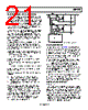
19 / 84 page  Data Sheet ADP1053 Rev. A | Page 19 of 84 The accurate ADC reading is used for CS2 overcurrent protection (OCP) and monitoring. For more information, see the CS2_A and CS2_B Accurate OCP Flags section and the CS2 (CS2_A/CS2_B) Readings section. SR FETs REVERSE CURRENT PROTECTION In synchronous rectification applications, reverse current may flow from VOUT through an output inductor, SR FETs, and a sense resistor to the power ground. If the SR FETs are kept on, the large reverse current can damage the SR FETs or the gate driver circuit under extreme conditions. SR FET reverse current protection is implemented using analog comparators. The reverse current protection threshold can be set using Register 0xFE84 and Register 0xFE85. If the voltage difference between CS2− and CS2+ is greater than the reverse current protection threshold programmed in these registers, the flag (REVERSE_A or REVERSE_B) is triggered. The action taken when the threshold is triggered can be programmed in Register 0xFE83. ADC ADP1053 VOUT CS2–_A/ CS2–_B CS2+_A/ CS2+_B 200µA 200µA REVERSE CURRENT PROTECTION THRESHOLD DEBOUNCE FLAG 12 BITS RSENSE Figure 17. SR FET Reverse Current Protection CONTROL LOOPS AND FEEDBACK REFERENCES Channel A and Channel B each have an independent voltage feedback control loop. The feedback uses the sensed signals from VS+_A and VS−_A (for Channel A) and VS+_B and VS−_B (for Channel B). Register 0xFE22 and Register 0xFE24 set the reference voltage for Channel A; Register 0xFE23 and Register 0xFE25 set the reference voltage for Channel B. Each LSB corresponds to the LSB of the VS_A/VS_B accurate ADC, which is 390.6 μV (see the VS_A and VS_B Readings section). The output voltage must be divided down using a resistor divider network (R1 and R2 in Figure 11) to set up a feedback voltage at the VS_A/VS_B pins. To convert the register value to an output voltage reference, use the following equation: VOUT = VS_Ref_Voltage_Value × 390.6 μV × (R1 + R2)/R2 For example, in a 12 V system with an 11 kΩ and 1 kΩ resistor divider, the reference voltage register value for Channel A is 0xB00 (2816 decimal). This register value is converted as follows: VOUT = 2816 × 390.6 μV × (11 kΩ + 1 kΩ)/1 kΩ = 13.2 V To prevent the writing of invalid voltage reference values to the registers, the value written to the registers does not take effect in the closed-loop operation until the GO command is executed. For Channel A, the GO command is executed by writing 1 to Bit 0 in Register 0xFE61. For Channel B, the GO command is executed by writing 1 to Bit 1 in Register 0xFE61. This function allows the user to read back and confirm the reference register value before implementing it for closed-loop operation. In addition, to prevent a channel from outputting a voltage that is outside its capability, Register 0xFE1E through Register 0xFE21 can be used to set the high and low limits for the feedback refer- ences. The reference registers can only be set to values between the low and high limits. If the user attempts to write a value that is out of range to the reference register, the value is ignored and the voltage setting error flag (VS_SET_ERR_A or VS_SET_ ERR_B) is set. Note that the VS_SET_ERR_x flag is set during the writing of the invalid value and is cleared when the write fails; the latched flag is also set but is not cleared. If the reference register value is not modified but the reference limit register is modified such that the reference is out of range, the write is successful. However, the reference value remains unchanged, and the VS_SET_ERR_x flag is set. VOLTAGE SETTING WITH SLEW RATE The ADP1053 provides a method for output voltage adjustment with slew rate control. The slew rate is set using Bits[3:1] of Register 0xFE86 (for VS_A) and Register 0xFE87 (for VS_B). The slew rate function is enabled by setting Bit 0 in Register 0xFE86 or Register 0xFE87. When a slew rate is enabled and the ADP1053 receives an output voltage adjustment command, the ADP1053 adjusts the voltage setting with the preset slew rate. |
|
ссылки URL |
| Вашему бизинису помогли Аллдатащит? [ DONATE ] |
Что такое Аллдатащит | реклама | контакт | Конфиденциальность | Ссылка на техническое описание | обмен ссыками | поиск по производителю All Rights Reserved©Alldatasheet.com |
| Russian : Alldatasheetru.com | Korean : Alldatasheet.co.kr | Spanish : Alldatasheet.es | French : Alldatasheet.fr | Italian : Alldatasheetit.com Portuguese : Alldatasheetpt.com | Polish : Alldatasheet.pl | Vietnamese : Alldatasheet.vn Indian : Alldatasheet.in | Mexican : Alldatasheet.com.mx | British : Alldatasheet.co.uk | New Zealand : Alldatasheet.co.nz |
|
Family Site : ic2ic.com |
icmetro.com |
 Russian ▼
 English
 Chinese
 German
 Japanese
 Russian
 Korean
 Spanish
 French
 Italian
 Portuguese
 Polish
 Vietnamese
 Indian
 Mexican
 British
 New Zealand