|
поискавой системы для электроныых деталей |
|
|
поискавой системы для электроныых деталей |
|
ADP1053ACPZ-R7 датащи(PDF) 73 Page - Analog Devices |
|
|
|||||||||||||||||||||||||||||
ADP1053ACPZ-R7 датащи(HTML) 73 Page - Analog Devices |
|
|
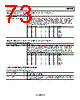
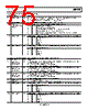
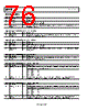
73 / 84 page  Data Sheet ADP1053 Rev. A | Page 73 of 84 Register 0xFE75 sets the OTP1 threshold value. The debounce time of the OTP1 flag is 100 ms. Table 110. Register 0xFE75—OTP1 Threshold Bits Bit Name R/W Description [7:0] OTP1 threshold R/W OTP1 threshold. This register, adding 0 as the MSB, results in a 9-bit threshold value. This 9-bit value is compared to the nine MSBs of the RTD1 value register (Register 0xFED7). If the OTP1 threshold is higher than the RTD1 ADC reading, the OTP1 flag is set. The eight bits of this register allow 256 threshold settings from 0 mV to 800 mV. One LSB corresponds to 800 mV/256 = 3.125 mV. However, threshold settings at the low end and the high end are not allowed. The valid range for this register value is 2 to 244 (decimal). Bit 7 Bit 6 … Bit 3 Bit 2 Bit 1 Bit 0 OTP1 Limit (mV) 0 0 … 0 0 1 0 6.25 … … … … … … … … 0 0 … 0 1 0 0 12.5 0 0 … 0 1 0 1 15.625 … … … … … … … … 1 1 … 0 0 1 1 459.375 1 1 … 0 1 0 0 762.5 Register 0xFE76 sets the OTP2 threshold value. The debounce time of the OTP2 flag is 100 ms. Table 111. Register 0xFE76—OTP2 Threshold Bits Bit Name R/W Description [7:0] OTP2 threshold R/W OTP2 threshold. This register, adding 0 as the MSB, results in a 9-bit threshold value. This 9-bit value is compared to the nine MSBs of the RTD2 value register (Register 0xFED8). If the OTP2 threshold is higher than the RTD2 ADC reading, the OTP2 flag is set. The eight bits of this register allow 256 threshold settings from 0 mV to 800 mV. One LSB corresponds to 800 mV/256 = 3.125 mV. However, threshold settings at the low end and the high end are not allowed. The valid range for this register value is 2 to 244 (decimal). Bit 7 Bit 6 … Bit 3 Bit 2 Bit 1 Bit 0 OTP2 Limit (mV) 0 0 … 0 0 1 0 6.25 … … … … … … … … 0 0 … 0 1 0 0 12.5 0 0 … 0 1 0 1 15.625 … … … … … … … … 1 1 … 0 0 1 1 459.375 1 1 … 0 1 0 0 762.5 ACSNS AND FEEDFORWARD SETTING REGISTERS Table 112. Register 0xFE77—ACSNS Gain Trim Bits Bit Name R/W Description 7 Trim polarity R/W 1 = negative gain is introduced. 0 = positive gain is introduced. [6:0] ACSNS trim R/W This value sets the amount of gain trim that is applied to the ACSNS ADC reading. This register trims the voltage at the ACSNS pin for external resistor tolerances. For more information, see the ACSNS Gain Trim section. |
|
ссылки URL |
| Вашему бизинису помогли Аллдатащит? [ DONATE ] |
Что такое Аллдатащит | реклама | контакт | Конфиденциальность | Ссылка на техническое описание | обмен ссыками | поиск по производителю All Rights Reserved©Alldatasheet.com |
| Russian : Alldatasheetru.com | Korean : Alldatasheet.co.kr | Spanish : Alldatasheet.es | French : Alldatasheet.fr | Italian : Alldatasheetit.com Portuguese : Alldatasheetpt.com | Polish : Alldatasheet.pl | Vietnamese : Alldatasheet.vn Indian : Alldatasheet.in | Mexican : Alldatasheet.com.mx | British : Alldatasheet.co.uk | New Zealand : Alldatasheet.co.nz |
|
Family Site : ic2ic.com |
icmetro.com |
 Russian ▼
 English
 Chinese
 German
 Japanese
 Russian
 Korean
 Spanish
 French
 Italian
 Portuguese
 Polish
 Vietnamese
 Indian
 Mexican
 British
 New Zealand