|
поискавой системы для электроныых деталей |
|
|
поискавой системы для электроныых деталей |
|
ADP1053ACPZ-R7 датащи(PDF) 58 Page - Analog Devices |
|
|
|||||||||||||||||||||||||||||
ADP1053ACPZ-R7 датащи(HTML) 58 Page - Analog Devices |
|
|
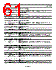
58 / 84 page  ADP1053 Data Sheet Rev. A | Page 58 of 84 Table 52. Register 0xFE1E—VS_A Reference Maximum Limit Bits Bit Name R/W Description [7:6] Reserved R/W Reserved. [5:0] VS_A maximum reference R/W This register sets the maximum limit of the Channel A output voltage reference. It sets the six MSBs for the reference limit. The factory default setting is 0x3F. Table 53. Register 0xFE1F—VS_B Reference Maximum Limit Bits Bit Name R/W Description [7:6] Reserved R/W Reserved. [5:0] VS_B maximum reference R/W This register sets the maximum limit of the Channel B output voltage reference. It sets the six MSBs for the reference limit. The factory default setting is 0x3F. Table 54. Register 0xFE20—VS_A Reference Minimum Limit Bits Bit Name R/W Description [7:6] Reserved R/W Reserved. [5:0] VS_A minimum reference R/W This register sets the minimum limit of the Channel A output voltage reference. It sets the six MSBs for the reference limit. The factory default setting is 0x00. Table 55. Register 0xFE21—VS_B Reference Minimum Limit Bits Bit Name R/W Description [7:6] Reserved R/W Reserved. [5:0] VS_B minimum reference R/W This register sets the minimum limit of the Channel B output voltage reference. It sets the six MSBs for the reference limit. The factory default setting is 0x00. Table 56. Register 0xFE22—VS_A Reference Setting (MSBs) Bits Bit Name R/W Description [7:0] VS_A voltage reference MSBs R/W This register sets the eight MSBs of the output voltage reference for Channel A. Together with Bits[3:0] of Register 0xFE24, this register sets the 12-bit reference. In a steady state, closed-loop operation, the output of the VS_A ADC is regulated to the reference setting value. Table 57. Register 0xFE23—VS_B Reference Setting (MSBs) Bits Bit Name R/W Description [7:0] VS_B voltage reference MSBs R/W This register sets the eight MSBs of the output voltage reference for Channel B. Together with Bits[3:0] of Register 0xFE25, this register sets the 12-bit reference. In a steady state, closed-loop operation, the output of the VS_B ADC is regulated to the reference setting value. Table 58. Register 0xFE24—VS_A Reference Setting (LSBs) Bits Bit Name R/W Description [7:4] Reserved R/W Reserved. [3:0] VS_A voltage reference LSBs R/W This register sets the four LSBs of the output voltage reference for Channel A. Together with Register 0xFE22, this register sets the 12-bit reference. In a steady state, closed-loop operation, the output of the VS_A ADC is regulated to the reference setting value. Table 59. Register 0xFE25—VS_B Reference Setting (LSBs) Bits Bit Name R/W Description [7:4] Reserved R/W Reserved. [3:0] VS_B voltage reference LSBs R/W This register sets the four LSBs of the output voltage reference for Channel B. Together with Register 0xFE23, this register sets the 12-bit reference. In a steady state, closed-loop operation, the output of the VS_B ADC is regulated to the reference setting value. |
|
ссылки URL |
| Вашему бизинису помогли Аллдатащит? [ DONATE ] |
Что такое Аллдатащит | реклама | контакт | Конфиденциальность | Ссылка на техническое описание | обмен ссыками | поиск по производителю All Rights Reserved©Alldatasheet.com |
| Russian : Alldatasheetru.com | Korean : Alldatasheet.co.kr | Spanish : Alldatasheet.es | French : Alldatasheet.fr | Italian : Alldatasheetit.com Portuguese : Alldatasheetpt.com | Polish : Alldatasheet.pl | Vietnamese : Alldatasheet.vn Indian : Alldatasheet.in | Mexican : Alldatasheet.com.mx | British : Alldatasheet.co.uk | New Zealand : Alldatasheet.co.nz |
|
Family Site : ic2ic.com |
icmetro.com |
 Russian ▼
 English
 Chinese
 German
 Japanese
 Russian
 Korean
 Spanish
 French
 Italian
 Portuguese
 Polish
 Vietnamese
 Indian
 Mexican
 British
 New Zealand