|
поискавой системы для электроныых деталей |
|
|
поискавой системы для электроныых деталей |
|
ADP1053ACPZ-R7 датащи(PDF) 29 Page - Analog Devices |
|
|
|||||||||||||||||||||||||||||
ADP1053ACPZ-R7 датащи(HTML) 29 Page - Analog Devices |
|
|
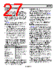
29 / 84 page  Data Sheet ADP1053 Rev. A | Page 29 of 84 The actions triggered by the CS_OCP, CS1_A_OCP, and CS1_B_OCP flags can be programmed with Register 0xFE00 and Register 0xFE04. For more information, see the Protection Actions section and the Flag Configuration Registers section. Cycle-by-Cycle Limit Function for SR Outputs In addition to the CS_OCP, CS1_A_OCP, and CS1_B_OCP flags, a cycle-by-cycle limit function can be used. This function is triggered by the CS, CS1_A, and CS1_B OCP comparator output. For example, when the CS OCP comparator output is high, all PWM outputs assigned to Channel C are disabled for the remainder of the switching cycle. The outputs are reenabled at the start of the next switching cycle. During a switching cycle, if the rising edge of a PWM output occurs after the flag is cleared, the PWM output is not disabled. To avoid current overstress of the body diode of the synchron- ous rectifiers, the cycle-by-cycle OCP actions of the SR PWM outputs (OUT3, OUT4, OUT7, and OUT8) can be programmed with Register 0xFE6D. The SR PWM outputs can be programmed the same way as other PWM outputs (see the CS, CS1_A, and CS1_B Fast OCP Flags section), or they can be programmed so that when an OCP condition occurs on the channel, the output is turned on. There is a 145 ns to 180 ns delay (dead time) between the comparator output going high and the turning on of the SR PWM outputs. The falling edge of the SR PWM outputs still follows the programmed value. Note that cycle-by-cycle protection is not affected by the flag time- out settings (the flag timeout values are set in Register 0xFE6F, Register 0xFE70, and Register 0xFE71). The comparator output can be completely ignored by setting Bit 7 in Register 0xFE6F, Register 0xFE70, and Register 0xFE71. CS2_A and CS2_B Accurate OCP Flags The CS2_A_OCP and CS2_B_OCP flags (Bit 4 in Register 0xFEC0 and Register 0xFEC1, respectively) are set when the current reading at CS2_A or CS2_B exceeds the threshold programmed in Register 0xFE18 and Register 0xFE19, respec- tively. A flag debounce time of 0 ms, 20 ms, 200 ms, or 1 sec can be set using Register 0xFE1A and Register 0xFE1B. Because the CS2_A/CS2_B reading is the average value over every 10 ms, there is an additional debounce and delay time of up to 10 ms. The response to the CS2_A_OCP and CS2_B_OCP flags can be programmed using Register 0xFE01. For more information, see the Protection Actions section and the Flag Configuration Registers section. OVERTEMPERATURE PROTECTION (OTP) AND OVERTEMPERATURE WARNING (OTW) FLAGS The ADP1053 provides overtemperature protection flags (OTP1 and OTP2) and overtemperature warning flags (OTW1 and OTW2) for each thermistor input, RTD1 and RTD2. The OTW1/ OTW2 flag is set when the temperature exceeds a programmable threshold above the OTP1/OTP2 threshold; the OTW1/OTW2 threshold can be set to 3.125 mV (1 LSB), 6.25 mV (2 LSBs), 9.375 mV (3 LSBs), or 12.5 mV (4 LSBs) using Register 0xFE8A. The OTW1/OTW2 flag is cleared when the temperature falls below the OTW1/OTW2 threshold. The OTW1/OTW2 flag can also be configured to activate the PGOOD_A/PGOOD_B flag using Bit 6 and Bit 2 in Register 0xFE8A. The OTW1 and OTW2 flags are Bits[3:2] of Register 0xFEC4. If the temperature sensed at the RTD1 pin exceeds the threshold programmed using Register 0xFE75, the OTP1 flag (Bit 3) is set in Register 0xFEC2. If the temperature sensed at the RTD2 pin exceeds the threshold programmed using Register 0xFE76, the OTP2 flag (Bit 4) is set in Register 0xFEC2. These flags are cleared when the OTP1/OTP2 condition is cleared, that is, when the temperature falls below the temperature threshold set in the OTW1/OTW2 settings register (Register 0xFE8A). The overtemperature hysteresis is the difference between the OTPx and OTWx temperature thresholds. Note that the threshold voltage is in inverse relationship to the temperature. Figure 27 illustrates the OTPx and OTWx temperature settings. OTWx FLAG IS SET OTPx FLAG IS SET TEMPERATURE VTH_OTWx > VTH_OTPx OTPx TEMPERATURE THRESHOLD OTWx TEMPERATURE THRESHOLD OT HYSTERESIS OTPx AND OTWx FLAGS ARE CLEARED TIME Figure 27. OTP, OTW, and OT Hysteresis The debounce time of the flag is fixed at 100 ms. Because the RTD1/RTD2 reading is the average value over every 10 ms, there is an additional debounce and delay time of up to 10 ms. The response to the OTP1/OTP2 flags can be programmed using Register 0xFE05. For more information, see the Protection Actions section and the Flag Configuration Registers section. The RTD trim is required to make accurate temperature readings at the lower end of the RTD ADC range. This results in a more accurate measurement for determining the OTP threshold (see the RTD1, RTD2, OTP1, and OTP2 Trim section). |
|
ссылки URL |
| Вашему бизинису помогли Аллдатащит? [ DONATE ] |
Что такое Аллдатащит | реклама | контакт | Конфиденциальность | Ссылка на техническое описание | обмен ссыками | поиск по производителю All Rights Reserved©Alldatasheet.com |
| Russian : Alldatasheetru.com | Korean : Alldatasheet.co.kr | Spanish : Alldatasheet.es | French : Alldatasheet.fr | Italian : Alldatasheetit.com Portuguese : Alldatasheetpt.com | Polish : Alldatasheet.pl | Vietnamese : Alldatasheet.vn Indian : Alldatasheet.in | Mexican : Alldatasheet.com.mx | British : Alldatasheet.co.uk | New Zealand : Alldatasheet.co.nz |
|
Family Site : ic2ic.com |
icmetro.com |
 Russian ▼
 English
 Chinese
 German
 Japanese
 Russian
 Korean
 Spanish
 French
 Italian
 Portuguese
 Polish
 Vietnamese
 Indian
 Mexican
 British
 New Zealand