|
поискавой системы для электроныых деталей |
|
|
поискавой системы для электроныых деталей |
|
ADP1053ACPZ-R7 датащи(PDF) 70 Page - Analog Devices |
|
|
|||||||||||||||||||||||||||||
ADP1053ACPZ-R7 датащи(HTML) 70 Page - Analog Devices |
|
|
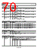
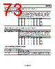
70 / 84 page  ADP1053 Data Sheet Rev. A | Page 70 of 84 Table 102. Register 0xFE6C—CS1_B Blanking Reference Edge Bits Bit Name R/W Description [7:4] Reserved R/W Reserved. 3 OUT6 rising edge blanking R/W This bit specifies whether the blanking time for the CS1_B OCP comparator is referenced to the rising edge of OUT6. 0 = no blanking at OUT6 rising edge. 1 = blanking time referenced to OUT6 rising edge. 2 OUT5 rising edge blanking R/W This bit specifies whether the blanking time for the CS1_B OCP comparator is referenced to the rising edge of OUT5. 0 = no blanking at OUT5 rising edge. 1 = blanking time referenced to OUT5 rising edge. 1 OUT2 rising edge blanking R/W This bit specifies whether the blanking time for the CS1_B OCP comparator is referenced to the rising edge of OUT2. 0 = no blanking at OUT2 rising edge. 1 = blanking time referenced to OUT2 rising edge. 0 OUT1 rising edge blanking R/W This bit specifies whether the blanking time for the CS1_B OCP comparator is referenced to the rising edge of OUT1. 0 = no blanking at OUT1 rising edge. 1 = blanking time referenced to OUT1 rising edge. Table 103. Register 0xFE6D—OUT3, OUT4, OUT7, and OUT8 Cycle-by-Cycle OCP Response Bits Bit Name R/W Description [7:4] Reserved R/W Reserved. 3 OUT8 cycle-by-cycle OCP response R/W When this bit is set, an OCP signal on the channel to which OUT8 is assigned causes OUT8 to turn on. The falling edge of the SR output still follows the programmed value. 2 OUT7 cycle-by-cycle OCP response R/W When this bit is set, an OCP signal on the channel to which OUT7 is assigned causes OUT7 to turn on. The falling edge of the SR output still follows the programmed value. 1 OUT4 cycle-by-cycle OCP response R/W When this bit is set, an OCP signal on the channel to which OUT4 is assigned causes OUT4 to turn on. The falling edge of the SR output still follows the programmed value. 0 OUT3 cycle-by-cycle OCP response R/W When this bit is set, an OCP signal on the channel to which OUT3 is assigned causes OUT3 to turn on. The falling edge of the SR output still follows the programmed value. Table 104. Register 0xFE6E—CS Gain Trim Bits Bit Name R/W Description 7 Gain polarity R/W 1 = negative gain is introduced. 0 = positive gain is introduced. [6:0] CS gain trim R/W This value calibrates the primary side current sense gain. For more information, see the CS, CS1_A, and CS1_B Gain Trim section. Table 105. Register 0xFE6F—CS OCP Settings Bits Bit Name R/W Description 7 CS OCP ignored R/W Setting this bit causes the CS OCP comparator output to be ignored. The flag is always cleared. These bits specify the blanking time. During this time, the CS OCP comparator output is ignored. The CS OCP blanking time is measured from OUT1 and OUT2. Bit 6 Bit 5 Bit 4 Leading Edge Blanking Time 0 0 0 0 ns 0 0 1 40 ns 0 1 0 80 ns 0 1 1 120 ns 1 0 0 200 ns 1 0 1 400 ns 1 1 0 600 ns [6:4] Leading edge blanking R/W 1 1 1 800 ns |
|
ссылки URL |
| Вашему бизинису помогли Аллдатащит? [ DONATE ] |
Что такое Аллдатащит | реклама | контакт | Конфиденциальность | Ссылка на техническое описание | обмен ссыками | поиск по производителю All Rights Reserved©Alldatasheet.com |
| Russian : Alldatasheetru.com | Korean : Alldatasheet.co.kr | Spanish : Alldatasheet.es | French : Alldatasheet.fr | Italian : Alldatasheetit.com Portuguese : Alldatasheetpt.com | Polish : Alldatasheet.pl | Vietnamese : Alldatasheet.vn Indian : Alldatasheet.in | Mexican : Alldatasheet.com.mx | British : Alldatasheet.co.uk | New Zealand : Alldatasheet.co.nz |
|
Family Site : ic2ic.com |
icmetro.com |
 Russian ▼
 English
 Chinese
 German
 Japanese
 Russian
 Korean
 Spanish
 French
 Italian
 Portuguese
 Polish
 Vietnamese
 Indian
 Mexican
 British
 New Zealand