|
поискавой системы для электроныых деталей |
|
|
поискавой системы для электроныых деталей |
|
ADP1053ACPZ-R7 датащи(PDF) 10 Page - Analog Devices |
|
|
|||||||||||||||||||||||||||||
ADP1053ACPZ-R7 датащи(HTML) 10 Page - Analog Devices |
|
|
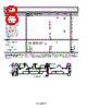
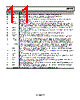
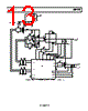
10 / 84 page  ADP1053 Data Sheet Rev. A | Page 10 of 84 PIN CONFIGURATION AND FUNCTION DESCRIPTIONS 1 VS+_A 2 VS–_A 3 PGND_A 4 OVP_A 5 CS2–_A 6 CS2+_A 7 PGOOD_A 8 CS1_A 9 ACSNS 10 PSON_A 23 CS1_B 24 PGOOD_B 25 CS2+_B 26 CS2–_B 27 OVP_B 28 PGND_B 29 VS–_B 30 VS+_B 22 CS 21 PSON_B ADP1053 TOP VIEW (Not to Scale) NOTES 1. THE EXPOSED PAD ON THE UNDERSIDE OF THE PACKAGE SHOULD BE SOLDERED TO AGND. Figure 4. Pin Configuration Table 4. Pin Function Descriptions Pin No. Mnemonic Description 1 VS+_A Noninverting Input of the Voltage Sense ADC for Channel A Loop Control. This signal is referenced to VS−_A. 2 VS−_A Inverting Input of the Voltage Sense ADC for Channel A Loop Control. There should be a low ohmic connection to AGND. 3 PGND_A Reference Pin for Channel A Overvoltage Protection (OVP_A). 4 OVP_A Overvoltage Protection Comparator Input for Channel A. This signal is referenced to PGND_A. 5 CS2−_A Inverting Input of the Differential Current Sense ADC for Channel A. The nominal voltage at this pin should be 1 V for optimal operation. 6 CS2+_A Noninverting Input of the Differential Current Sense ADC for Channel A. The nominal voltage at this pin should be 1 V for optimal operation. 7 PGOOD_A Power-Good Output (Open-Drain) for Channel A. This signal is referenced to AGND. This pin is controlled by the PGOOD_A flag and is driven low when the flag is set. The PGOOD_A flag is set when the POWER_SUPPLY_A, UVP_A, EEPROM_CRC, or SOFTSTART_FILTER_A flag is set. The ACSNS and OTW1 flags can also be programmed to be included. 8 CS1_A CS1 ADC Input and Fast Current Sense Input for Channel A. This signal is referenced to AGND. 9 ACSNS AC Sense ADC and Feedforward Operation Input. This pin is connected upstream of the main inductor through a resistor divider network. The nominal voltage at this pin should be 1 V. This signal is referenced to AGND. 10 PSON_A Power Supply On Input for Channel A. This signal is referenced to AGND. 11 OUT1 OUT1 PWM Logic Output Drive. This pin is connected to the input of a FET driver; it can be disabled when not in use. This signal is referenced to AGND. 12 OUT2 OUT2 PWM Logic Output Drive. This pin is connected to the input of a FET driver; it can be disabled when not in use. This signal is referenced to AGND. 13 OUT3 OUT3 PWM Logic Output Drive. This pin is connected to the input of a FET driver; it can be disabled when not in use. This signal is referenced to AGND. 14 OUT4 OUT4 PWM Logic Output Drive. This pin is connected to the input of a FET driver; it can be disabled when not in use. This signal is referenced to AGND. 15 OUT5 OUT5 PWM Logic Output Drive. This pin is connected to the input of a FET driver; it can be disabled when not in use. This signal is referenced to AGND. 16 OUT6 OUT6 PWM Logic Output Drive. This pin is connected to the input of a FET driver; it can be disabled when not in use. This signal is referenced to AGND. 17 OUT7 OUT7 PWM Logic Output Drive. This pin is connected to the input of a FET driver; it can be disabled when not in use. This signal is referenced to AGND. 18 OUT8 OUT8 PWM Logic Output Drive. This pin is connected to the input of a FET driver; it can be disabled when not in use. This signal is referenced to AGND. |
|
ссылки URL |
| Вашему бизинису помогли Аллдатащит? [ DONATE ] |
Что такое Аллдатащит | реклама | контакт | Конфиденциальность | Ссылка на техническое описание | обмен ссыками | поиск по производителю All Rights Reserved©Alldatasheet.com |
| Russian : Alldatasheetru.com | Korean : Alldatasheet.co.kr | Spanish : Alldatasheet.es | French : Alldatasheet.fr | Italian : Alldatasheetit.com Portuguese : Alldatasheetpt.com | Polish : Alldatasheet.pl | Vietnamese : Alldatasheet.vn Indian : Alldatasheet.in | Mexican : Alldatasheet.com.mx | British : Alldatasheet.co.uk | New Zealand : Alldatasheet.co.nz |
|
Family Site : ic2ic.com |
icmetro.com |
 Russian ▼
 English
 Chinese
 German
 Japanese
 Russian
 Korean
 Spanish
 French
 Italian
 Portuguese
 Polish
 Vietnamese
 Indian
 Mexican
 British
 New Zealand