|
поискавой системы для электроныых деталей |
|
|
поискавой системы для электроныых деталей |
|
ADP1053ACPZ-R7 датащи(PDF) 65 Page - Analog Devices |
|
|
|||||||||||||||||||||||||||||
ADP1053ACPZ-R7 датащи(HTML) 65 Page - Analog Devices |
|
|
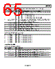
65 / 84 page  Data Sheet ADP1053 Rev. A | Page 65 of 84 Table 89. Register 0xFE43/0xFE47/0xFE4B/0xFE4F/0xFE53/0xFE57/0xFE5B/0xFE5F—OUT1 to OUT8 Settings Bits Bit Name R/W Description 7 OUTX 180° delay R/W Setting this bit adds a 180° delay to the timing of the OUTX edges. These bits assign the PWM output to a channel (OUTX = OUT1, OUT2, OUT3, OUT4, OUT5, OUT6, OUT7, or OUT8). Bit 6 Bit 5 PWM Output Assignment 0 0 OUTX assigned to Channel A. 0 1 OUTX assigned to Channel B. 1 0 OUTX assigned to Channel C with soft start enabled. [6:5] Channel assignment R/W 1 1 OUTX assigned to Channel C with soft start disabled. 4 Current/volt-second balance enable R/W If current balance control or volt-second balance control is enabled, this bit enables the feature on the specific PWM output (OUTX = OUT1, OUT2, OUT3, OUT4, OUT5, OUT6, OUT7, or OUT8). 0 = OUTX modulated by volt-second balance control. 1 = OUTX modulated by dual-phase current balance control. 3 tRX modulation enable R/W 0 = no PWM modulation of the tRX edge. 1 = PWM modulation acts on the tRX edge. 2 tRX modulation sign R/W 0 = positive sign. Increase of PWM modulation moves tRX right. 1 = negative sign. Increase of PWM modulation moves tRX left. 1 tFX modulation enable R/W 0 = no PWM modulation of the tFX edge. 1 = PWM modulation acts on the tFX edge. 0 tFX modulation sign R/W 0 = positive sign. Increase of PWM modulation moves tFX right. 1 = negative sign. Increase of PWM modulation moves tFX left. Table 90. Register 0xFE60—PWM Output Pin Disable Bits Bit Name R/W Description 7 OUT8 disable R/W Setting this bit disables the OUT8 output. 6 OUT7 disable R/W Setting this bit disables the OUT7 output. 5 OUT6 disable R/W Setting this bit disables the OUT6 output. 4 OUT5 disable R/W Setting this bit disables the OUT5 output. 3 OUT4 disable R/W Setting this bit disables the OUT4 output. 2 OUT3 disable R/W Setting this bit disables the OUT3 output. 1 OUT2 disable R/W Setting this bit disables the OUT2 output. 0 OUT1 disable R/W Setting this bit disables the OUT1 output. GO COMMAND REGISTER Table 91. Register 0xFE61—GO Commands Bits Bit Name R/W Description [7:4] Reserved R/W Reserved. 3 Frequency GO R/W This bit synchronously latches the contents of Register 0xFE0A to Register 0xFE0C into the shadow registers used to calculate the switching frequency. 2 PWM setting GO R/W This bit synchronously latches the contents of Register 0xFE40 to Register 0xFE5F into the shadow registers used to calculate the PWM edge timing. 1 VS_B reference GO R/W This bit synchronously latches the contents of Register 0xFE23 and Register 0xFE25 into the shadow registers used to calculate the VS_B voltage reference. 0 VS_A reference GO R/W This bit synchronously latches the contents of Register 0xFE22 and Register 0xFE24 into the shadow registers used to calculate the VS_A voltage reference. |
|
ссылки URL |
| Вашему бизинису помогли Аллдатащит? [ DONATE ] |
Что такое Аллдатащит | реклама | контакт | Конфиденциальность | Ссылка на техническое описание | обмен ссыками | поиск по производителю All Rights Reserved©Alldatasheet.com |
| Russian : Alldatasheetru.com | Korean : Alldatasheet.co.kr | Spanish : Alldatasheet.es | French : Alldatasheet.fr | Italian : Alldatasheetit.com Portuguese : Alldatasheetpt.com | Polish : Alldatasheet.pl | Vietnamese : Alldatasheet.vn Indian : Alldatasheet.in | Mexican : Alldatasheet.com.mx | British : Alldatasheet.co.uk | New Zealand : Alldatasheet.co.nz |
|
Family Site : ic2ic.com |
icmetro.com |
 Russian ▼
 English
 Chinese
 German
 Japanese
 Russian
 Korean
 Spanish
 French
 Italian
 Portuguese
 Polish
 Vietnamese
 Indian
 Mexican
 British
 New Zealand