|
поискавой системы для электроныых деталей |
|
|
поискавой системы для электроныых деталей |
|
ADP1055ACPZ-R7 датащи(PDF) 117 Page - Analog Devices |
|
|
|||||||||||||||||||||||||||||
ADP1055ACPZ-R7 датащи(HTML) 117 Page - Analog Devices |
|
|
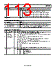
117 / 140 page  Data Sheet ADP1055 Rev. A | Page 117 of 140 Table 203. Register 0xFE5B—AUTO_GO_CMD Bits Bit Name R/W Description [7:2] Reserved R Reserved. 1 Frequency auto-go enable R/W 0 = GO_CMD, Bit 2 (Register 0xFE00) is required to latch the programmed frequency in FREQUENCY_SWITCH into the internal loop frequency. 1 = write to FREQUENCY_SWITCH is automatically latched into the internal loop switching frequency. 0 VREF auto-go enable R/W 0 = GO_CMD, Bit 0 (Register 0xFE00) is required to latch the programmed reference voltage in VOUT_COMMAND into the internal loop frequency. 1 = write to any commands affecting the reference voltage is automatically latched into the internal loop reference voltage. Commands that affect the reference voltage include VOUT_COMMAND, VOUT_MODE, VOUT_MAX, VOUT_TRIM, VOUT_CAL_OFFSET, VOUT_SCALE_LOOP, and VOUT_DROOP. Table 204. Register 0xFE5C—DIODE_EMULATION Bits Bit Name R/W Description [7:5] SR debounce R/W These bits delay the onset of LLM or CCM when the light load mode or deep light load mode threshold is crossed. The device transitions from CCM to LLM based on the debounce time specified using these bits and the light load mode threshold. The same is true when the device transitions from LLM to CCM and is also valid for deep light load mode. For example, if the device is in CCM and the load current step places the device in LLM, the device physically enters LLM, that is, the SR outputs start phasing after the debounce time set by these bits. The same debounce time delays the entry to DCM. Entering deep light load mode is possible only if the ADP1055 is already in DCM (that is, the device is already below the DCM threshold) and SR transitioning is finished. Bit 7 Bit 6 Bit 5 Debounce Time (tSW) 0 0 0 0 0 0 1 64 0 1 0 128 0 1 1 256 1 0 0 512 1 0 1 768 1 1 0 1152 1 1 1 2048 [4:2] Reserved R Reserved. 1 Diode emulation mode R/W 0 = disable diode emulation mode (SR LLM and deep LLM are active if the thresholds are correctly set). 1 = enable diode emulation mode (SR LLM setting is disabled. Only deep LLM is active if the threshold is correctly set). Once the SR outputs are disabled upon a negative going zero crossing transition, they are disabled for a period of 327 μs to 754 μs to ensure that the comparator is not falsely triggered. 0 SR toggle rate in diode emulation mode R/W 0 = SR outputs toggle once in one tSW. 1 = SR outputs toggle twice in one tSW (recommended setting). Table 205. Register 0xFE5D—CS2_CONST_CUR_MODE Bits Bit Name R/W Description [7:6] Reserved R Reserved. [5:4] Slew rate during CC mode (turbo mode only) R/W 00 = Nominal slew rate of (8 × 1.18) V/sec Setting 00 provides 2x nominal at VS± pins in CC turbo mode 01 = 16× 10 = 24× 11 = 32× 3 CC mode thresholds polarity R/W 0 = positive (% above OCP limit) 1 = negative (% below OCP limit) |
|
ссылки URL |
| Вашему бизинису помогли Аллдатащит? [ DONATE ] |
Что такое Аллдатащит | реклама | контакт | Конфиденциальность | Ссылка на техническое описание | обмен ссыками | поиск по производителю All Rights Reserved©Alldatasheet.com |
| Russian : Alldatasheetru.com | Korean : Alldatasheet.co.kr | Spanish : Alldatasheet.es | French : Alldatasheet.fr | Italian : Alldatasheetit.com Portuguese : Alldatasheetpt.com | Polish : Alldatasheet.pl | Vietnamese : Alldatasheet.vn Indian : Alldatasheet.in | Mexican : Alldatasheet.com.mx | British : Alldatasheet.co.uk | New Zealand : Alldatasheet.co.nz |
|
Family Site : ic2ic.com |
icmetro.com |
 Russian ▼
 English
 Chinese
 German
 Japanese
 Russian
 Korean
 Spanish
 French
 Italian
 Portuguese
 Polish
 Vietnamese
 Indian
 Mexican
 British
 New Zealand