|
поискавой системы для электроныых деталей |
|
|
поискавой системы для электроныых деталей |
|
ADP1055ACPZ-R7 датащи(PDF) 36 Page - Analog Devices |
|
|
|||||||||||||||||||||||||||||
ADP1055ACPZ-R7 датащи(HTML) 36 Page - Analog Devices |
|
|
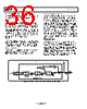
36 / 140 page  ADP1055 Data Sheet Rev. A | Page 36 of 140 Digital Share Bus Scheme Each power supply compares the digital word that it is outputting with the digital words of all the other supplies on the bus. Round 1 In Round 1, every supply first places its MSB on the bus. If a supply senses that its MSB is the same as the value on the bus, it continues to Round 2. If a supply senses that its MSB is less than the value on the bus, it means that this supply must be a slave. When a supply becomes a slave, it stops communicating on the share bus because it knows that it is not the master. The supply then increases its output voltage in an attempt to share more current. If two units have the same MSB, they both continue to Round 2 because either of them may be the master. Round 2 In Round 2, all supplies that are still communicating on the bus place their second MSB on the share bus. If a supply senses that its MSB is less than the value on the bus, it means that this supply must be a slave and it stops communicating on the share bus. Round 3 to Round 8 The same algorithm is repeated for up to eight rounds to allow supplies to compare their digital words and, in this way, to determine whether each unit is the master or a slave. Digital Share Bus Configuration The digital share bus can be configured in various ways. The bandwidth of the share bus loop is programmable in Register 0xFE2B[2:0]. The extent to which a slave tries to match the current of the master is programmable in Register 0xFE2A[3:0]. The slave moves up 1 LSB for every share bus transaction (eight data bits plus start and stop bits; see the description of Register 0xFE2B in Table 156). The master moves down x LSBs per share bus transaction, where x is the share bus setting in Register 0xFE2A[7:4]. The maximum limit for the output voltage of the slave is 400 mV at the VS± pins. The ISHARE_FAULT is set when the current share loop reaches its maximum value, that is, 400 mV at the VS± pins. It is recommended that there be a load line of 5 mΩ to 10 mΩ between the output terminals of the power supply to the load. DROOP SHARING The droop sharing functionality is implemented using the VOUT_DROOP command (Register 0x28). Using this command, a fixed amount of load line in mV/A can be applied to the output voltage. The output voltage is continuously sampled with a selectable rate (set in Register 0xFE65[1:0]) before the droop is applied. Under droop current sharing, the output voltage changes at a rate determined by the VOUT_TRANSITION_ RATE command. Setting 0xFE65[2] = 1 changes the internal voltage reference to the fastest internal supported rate. Figure 61. How the Share Bus Generates the Digital Word to Place on the Digital Share Bus CURRENT SENSE ADC 1 LSB = 29.3µV 35mV/29.3µV = 1195 MASTER + 35mV – DIGITAL WORD DIGITAL FILTER ÷16 12 BITS 1195 DEC 0x4AB 8 BITS 74 DEC 0x4A 0x4A CS2+ CS2– VDD SHARE BUS 8-BIT WORD 0xB5 8-BIT WORD 0x4A ISHARE IOUT = 35A 1mΩ PSU A |
|
ссылки URL |
| Вашему бизинису помогли Аллдатащит? [ DONATE ] |
Что такое Аллдатащит | реклама | контакт | Конфиденциальность | Ссылка на техническое описание | обмен ссыками | поиск по производителю All Rights Reserved©Alldatasheet.com |
| Russian : Alldatasheetru.com | Korean : Alldatasheet.co.kr | Spanish : Alldatasheet.es | French : Alldatasheet.fr | Italian : Alldatasheetit.com Portuguese : Alldatasheetpt.com | Polish : Alldatasheet.pl | Vietnamese : Alldatasheet.vn Indian : Alldatasheet.in | Mexican : Alldatasheet.com.mx | British : Alldatasheet.co.uk | New Zealand : Alldatasheet.co.nz |
|
Family Site : ic2ic.com |
icmetro.com |
 Russian ▼
 English
 Chinese
 German
 Japanese
 Russian
 Korean
 Spanish
 French
 Italian
 Portuguese
 Polish
 Vietnamese
 Indian
 Mexican
 British
 New Zealand