|
поискавой системы для электроныых деталей |
|
|
поискавой системы для электроныых деталей |
|
ADP1055ACPZ-R7 датащи(PDF) 21 Page - Analog Devices |
|
|
|||||||||||||||||||||||||||||
ADP1055ACPZ-R7 датащи(HTML) 21 Page - Analog Devices |
|
|
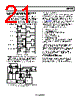
21 / 140 page  Data Sheet ADP1055 Rev. A | Page 21 of 140 PWM AND SYNCHRONOUS RECTIFIER OUTPUTS (OUTA, OUTB, OUTC, OUTD, SR1, SR2) The PWM and SR outputs are used for control of the primary side drivers and the synchronous rectifier drivers. These outputs can be used for several control topologies, such as full-bridge, phase-shifted ZVS configurations and interleaved, two switch forward converter configurations. Delays between the rising and falling edges can be individually programmed (see Figure 24). Figure 24. PWM Timing Diagram Take special care to avoid shoot-through and cross-conduction. It is recommended that the software GUI be used to program these outputs. Figure 25 shows an example configuration to drive a full-bridge topology with synchronous rectification. Figure 25. PWM Pin Assignment for Full-Bridge, Phase-Shifted Topology with Synchronous Rectification Go and Auto Go Command The PWM outputs (OUTA to OUTD) and the SR outputs (SR1 and SR2) are all synchronized with each other. Therefore, when reprogramming more than one of these outputs, it is important to first update all the registers and then latch the information into the ADP1055 at the same time. This simultaneous updating of the PWM outputs is facilitated by the GO command (Register 0xFE00). The GO command acts as a gate to apply all functions related to the commands at the same time. The GO command gates the following functions: Frequency synchronization Line voltage feedforward Double update rate, volt-second balance Digital filter settings Frequency and PWM settings Voltage reference change During reprogramming, the outputs are temporarily disabled. It is recommended that the PWM outputs be disabled when not in use. The PMBus allows the user to change the voltage setting and the switching frequency on-the-fly. The auto go command (Register 0xFE5B) is an added level of protection that restricts the user from making a change to certain commands (see Table 203). For more information about the various programmable switching frequencies and PWM timings, see the Switching Frequency Programming section. SYNCHRONOUS RECTIFICATION SR1 and SR2 are recommended for use as the PWM control signals when using synchronous rectification. These PWM signals can be configured much like the other PWM outputs. t2 t4 t1 t5 t11 t7 t8 t10 tPERIOD tPERIOD t9 t6 t3 t12 PWM1 (OUTA) PWM2 (OUTB) PWM3 (OUTC) PWM4 (OUTD) SYNC RECT 1 (SR1) SYNC RECT 2 (SR2) ISOLATOR DRIVER DRIVER OUTA OUTB OUTC OUTD SR1 SR2 VIN OUTA OUTD OUTC OUTB SR1 SR2 |
|
ссылки URL |
| Вашему бизинису помогли Аллдатащит? [ DONATE ] |
Что такое Аллдатащит | реклама | контакт | Конфиденциальность | Ссылка на техническое описание | обмен ссыками | поиск по производителю All Rights Reserved©Alldatasheet.com |
| Russian : Alldatasheetru.com | Korean : Alldatasheet.co.kr | Spanish : Alldatasheet.es | French : Alldatasheet.fr | Italian : Alldatasheetit.com Portuguese : Alldatasheetpt.com | Polish : Alldatasheet.pl | Vietnamese : Alldatasheet.vn Indian : Alldatasheet.in | Mexican : Alldatasheet.com.mx | British : Alldatasheet.co.uk | New Zealand : Alldatasheet.co.nz |
|
Family Site : ic2ic.com |
icmetro.com |
 Russian ▼
 English
 Chinese
 German
 Japanese
 Russian
 Korean
 Spanish
 French
 Italian
 Portuguese
 Polish
 Vietnamese
 Indian
 Mexican
 British
 New Zealand