|
поискавой системы для электроныых деталей |
|
|
поискавой системы для электроныых деталей |
|
ADP1055ACPZ-R7 датащи(PDF) 33 Page - Analog Devices |
|
|
|||||||||||||||||||||||||||||
ADP1055ACPZ-R7 датащи(HTML) 33 Page - Analog Devices |
|
|
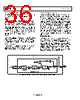
33 / 140 page  Data Sheet ADP1055 Rev. A | Page 33 of 140 Entering the Key Code The key code is a unique 32-bit pass code that is entered using the KEY_CODE command (Register 0xD7). Because this com- mand is a block read/block write command, the first data byte of this command is the number of bytes (4). When entering the key code, the data has this format: {0x04, KeyCode[7:0], KeyCode[15:8], KeyCode[23:16], KeyCode[31:17]}. (Note the low byte to high byte order of the 32-bit key code.) After the correct key code is entered, the user has full write access to all commands, including PMBus and manufacturer specific com- mands such as CMD_MASK (Register 0xF4) and EXTCMD_ MASK (Register 0xF5), which can be used to disable other commands using the command masking feature. The key code is also needed to change the EEPROM password (Register 0xD5). Command Mask The command mask feature allows any PMBus command or manufacturer specific command to be masked in the ADP1055. If the command is masked, a read or a write to that command results in a no acknowledge (NACK). PMBus commands are masked using Register 0xF4; manufacturer specific commands are masked using Register 0xF5. Using command masking, the user can block access to certain commands—such as commands that configure the switching frequency, the digital compensator, or the output voltage setpoint—while allowing access to the readback commands (READ_x, where x = IOUT, IN, VOUT, VIN, and so on). The SLV_ADDR_SELECT (Register 0xD0), EEPROM_PASSWORD (Register 0xD5), KEY_CODE (Register 0xD7), EEPROM_INFO (Register 0xF1), CMD_MASK (Register 0xF4), and EXTCMD_MASK (Register 0xF5) commands are not maskable. It is recommended that the ADP1055 GUI be used to configure the masking function (see Figure 53). Figure 53. Snapshot of the GUI Showing Lock and Unlock of Commands Changing the Key Code To change the key code, first unlock the EEPROM as described in the Unlock the EEPROM section. 1. After the EEPROM is unlocked, enter the 32-bit key code (default key code is 0xFFFFFFFF) using the KEY_CODE command (Register 0xD7). 2. Enter the new key code using the same command, for example, 0x1FEEDBAC (a pneumonic for negative feedback in twos complement format). 3. The key code is now changed to the new key code. Save the new key code into the user settings page of the EEPROM using the STORE_USER_ALL command (Register 0x15). SR PHASE-IN, SR TRANSITION, AND SR FAST PHASE-IN The SR1 and SR2 outputs are recommended for use as the PWM control signals when using synchronous rectification for the output (or secondary) rectifiers. These PWM signals can be configured similar to other PWM outputs. Figure 54. Example of SR Outputs in Light Load Mode (LLM) Figure 55. Example of SR Outputs in Heavy Load (CCM) When the mode changes from LLM to CCM, an abrupt change in the SR outputs may cause the output voltage to dip momentarily. An optional SR transition process (during which the pulse width of the SR PWM outputs is increased slowly) can be applied to the SR1 and SR2 outputs. The SR transition can be enabled by setting Register 0xFE50[5]. The speed at which the SR edges move from zero duty cycle to maximum duty cycle (as determined by the control loop) can be programmed from 5 ns per tSW to 5 ns per 1024 tSW (tSW = switching cycle) using Register 0xFE5F[7:4]. OUTPUT VOLTAGE SLEW RATE The output voltage slew rate (or transition rate) can be set using the PMBus VOUT_TRANSITION_RATE command (Register 0x27). The slew rate determines how quickly the output voltage is adjusted in response to a change in the digital reference. The fastest slew rate supported by the ADP1055 is 1 kV/sec, and the slowest rate is 14.3 V/sec. A PMBus command setting of 0 sets the slew rate to the slowest setting. This slew rate is the rate that the internal setpoint reference can change; the actual change of the output voltage depends on the bandwidth of the control loop and its ability to track the reference. The VOUT_TRANSITION_RATE command can be disabled using Register 0xFE65[2]. ADAPTIVE DEAD TIME COMPENSATION Register 0xFE1D to Register 0xFE24 are the adaptive dead time (ADT) registers. These registers allow the dead time between |
|
ссылки URL |
| Вашему бизинису помогли Аллдатащит? [ DONATE ] |
Что такое Аллдатащит | реклама | контакт | Конфиденциальность | Ссылка на техническое описание | обмен ссыками | поиск по производителю All Rights Reserved©Alldatasheet.com |
| Russian : Alldatasheetru.com | Korean : Alldatasheet.co.kr | Spanish : Alldatasheet.es | French : Alldatasheet.fr | Italian : Alldatasheetit.com Portuguese : Alldatasheetpt.com | Polish : Alldatasheet.pl | Vietnamese : Alldatasheet.vn Indian : Alldatasheet.in | Mexican : Alldatasheet.com.mx | British : Alldatasheet.co.uk | New Zealand : Alldatasheet.co.nz |
|
Family Site : ic2ic.com |
icmetro.com |
 Russian ▼
 English
 Chinese
 German
 Japanese
 Russian
 Korean
 Spanish
 French
 Italian
 Portuguese
 Polish
 Vietnamese
 Indian
 Mexican
 British
 New Zealand