|
поискавой системы для электроныых деталей |
|
|
поискавой системы для электроныых деталей |
|
ADP1055ACPZ-R7 датащи(PDF) 37 Page - Analog Devices |
|
|
|||||||||||||||||||||||||||||
ADP1055ACPZ-R7 датащи(HTML) 37 Page - Analog Devices |
|
|
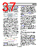
37 / 140 page  Data Sheet ADP1055 Rev. A | Page 37 of 140 LIGHT LOAD MODE AND DEEP LIGHT LOAD MODE To facilitate a reduction of power loss at light loads, the ADP1055 supports light load mode and deep light load mode. The threshold, speed, and hysteresis for deep light load mode are selectable in Register 0xFE4B. In deep light load mode, a selectable set of PWM outputs can be disabled using Register 0xFE4C. Typical examples include shutting down the synchronous rectifiers or shutting down certain PWM outputs in an interleaved topology for phase shedding. Figure 62. Light Load Settings in the GUI The threshold, speed, and hysteresis for light load mode are programmed in Register 0xFE5F. In SR light load mode (SR LLM), the synchronous rectifiers operate in the forward conduction mode only; that is, they are turned off during the freewheeling period of the switching period in a buck derived isolated topology (either half wave or full wave rectifier on the output). In this way, the loss associated with the diode drop of the MOSFET is minimized by turning the channel of the MOSFET on, as well as maintaining the output inductor in discontinuous conduction mode (DCM). The rising and falling edges of the synchronous rectifiers in SR LLM are programmed in Register 0xFE19 to Register 0xFE1C. When entering SR LLM from SR normal mode or deep LLM, or when exiting SR LLM to SR normal mode based on the hysteresis level, the SR edges move as programmed by the phase-in speed in Register 0xFE5F[7:4]. The SR LLM settings (Register 0xFE19 to Register 0xFE1C) determine the minimum and maximum rising and falling edges of the SR PWM outputs in SR LLM mode. If the load demands a duty cycle between the minimum and maximum settings, the SR edges are adjusted according to the required duty cycle for OUTA to OUTD. To enable the deep light load mode, the light load mode threshold must be greater than zero. Figure 63. Overlay of All SR Modes PULSE SKIPPING The ADP1055 supports a pulse skipping mode in which a PWM pulse is not turned on for the entire switching period. Pulse skipping can be activated by setting Register 0xFE50[1] = 1. The ADP1055 enters pulse skipping mode when the required duty cycle is less than the modulation value set in Register 0xFE53. Register 0xFE50[0] = 0 sets all modulated edges to the start of the switching period. In the case of negative edge modulation, this setting can cause the PWM outputs to be inverted; therefore, setting Register 0xFE50[0] = 1 programs the device to make the PWM outputs = 0 V in pulse skipping. For topologies such as the full-bridge phase shifted topology, where two PWM outputs are on without modulation for half the switching period, the setting in Register 0xFE50[4] allows the ADP1055 to disable such PWM outputs whether modulation is enabled or not. SOFT STOP The ADP1055 supports soft stop functionality. Soft stop can be enabled for normal shutdown of the power supply using the OPERATION and ON_OFF_CONFIG commands, as described in the Power-Up and Power-Down section. Soft stop can also be enabled during a fault triggered condition using Register 0xFE51[7:6]. The soft stop time is programmed using the TOFF_DELAY and TOFF_FALL commands (Register 0x64 and Register 0x65). During soft stop, various faults such as OTP, OVP, and GPIO faults can be masked using Register 0xFE47. To maintain a zero output voltage, the SR1 and SR2 PWM outputs can be programmed to stay on for an additional time (see the description of Register 0xFE50[7:6] in Table 193). DUTY CYCLE DOUBLE UPDATE RATE The ADP1055 senses the output voltage just before the beginning of the switching period and, depending on the error voltage, the next duty cycle command is initiated. Because a transient condition can occur at any time between switching periods, the one-cycle update of the duty cycle causes a phase loss that is equal to Φ = 360 × (td × fC) where: td is the combined delay of the ADC sampling plus the loop calculations for the compensator plus any additional propagation delay. fC is the crossover frequency. The minimum delay for the system is D × tSW because it is only after D × tSW that the effect of the duty cycle command takes place. Due to this phase loss (which increases as the crossover frequency approaches the switching frequency), the crossover frequency of the system cannot be widened with satisfactory phase margin. To reduce the phase loss, the ADP1055 uses a double update rate for the duty cycle, whereby the output voltage is sampled just before half the switching period and the new duty cycle command is issued. In this way, the phase loss from two subsequent duty cycle commands is halved to D × tSW/2. Duty cycle double update rate is optional and is enabled by setting Register 0xFE57[0] = 1. When using the duty cycle double update rate, it is recommended that duty balance also be enabled (Register 0xFE57[7] = 1). |
|
ссылки URL |
| Вашему бизинису помогли Аллдатащит? [ DONATE ] |
Что такое Аллдатащит | реклама | контакт | Конфиденциальность | Ссылка на техническое описание | обмен ссыками | поиск по производителю All Rights Reserved©Alldatasheet.com |
| Russian : Alldatasheetru.com | Korean : Alldatasheet.co.kr | Spanish : Alldatasheet.es | French : Alldatasheet.fr | Italian : Alldatasheetit.com Portuguese : Alldatasheetpt.com | Polish : Alldatasheet.pl | Vietnamese : Alldatasheet.vn Indian : Alldatasheet.in | Mexican : Alldatasheet.com.mx | British : Alldatasheet.co.uk | New Zealand : Alldatasheet.co.nz |
|
Family Site : ic2ic.com |
icmetro.com |
 Russian ▼
 English
 Chinese
 German
 Japanese
 Russian
 Korean
 Spanish
 French
 Italian
 Portuguese
 Polish
 Vietnamese
 Indian
 Mexican
 British
 New Zealand