|
поискавой системы для электроныых деталей |
|
|
поискавой системы для электроныых деталей |
|
ADP1055ACPZ-R7 датащи(PDF) 35 Page - Analog Devices |
|
|
|||||||||||||||||||||||||||||
ADP1055ACPZ-R7 датащи(HTML) 35 Page - Analog Devices |
|
|
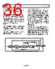
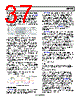
35 / 140 page  Data Sheet ADP1055 Rev. A | Page 35 of 140 Digital Share Bus The digital share bus scheme is similar in principle to the tradi- tional analog share bus scheme. The difference is that instead of using a voltage on the share bus to represent current, a digital word is used. The ADP1055 outputs a digital word onto the share bus. The digital word is a function of the current that the power supply is providing (the higher the current, the larger the digital word). The power supply with the highest current controls the bus (master). A power supply that is putting out less current (slave) sees that another supply is providing more power to the load than it is. During the next cycle, the slave increases its current output contri- bution by increasing its output voltage. This cycle continues until the slave outputs the same current as the master, within a programmable tolerance range. Figure 58 shows the configu- ration of the digital share bus. Figure 58. Digital Current Share Configuration The digital share bus is based on a single-wire communication bus principle; that is, the clock and data signals are contained together. When two or more ADP1055 devices are connected, they syn- chronize their share bus timing. This synchronization is performed by the start bit at the beginning of a communications frame. If a new ADP1055 is hot-swapped onto an existing digital share bus, the device waits to begin sharing until the next frame. The new ADP1055 monitors the share bus until it sees a stop bit, which designates the end of a share frame. It then performs synchroni- zation with the other ADP1055 devices during the next start bit. The digital share bus frame is shown in Figure 60. Figure 59 shows the possible signals on the share bus. Figure 59. Share Bus High, Low, and Idle Bits The length of a bit (tBIT) is fixed at 10 μs. A Logic 1 is defined as a high-to-low transition at the start of the bit and a low-to-high transition at 75% of tBIT. A Logic 0 is defined as a high-to-low transition at the start of the bit and a low-to-high transition at 25% of tBIT. The bus is idle when it is high during the whole period of tBIT. All other activity on the bus is illegal. Glitches up to tGLITCH (200 ns) are ignored. The digital word that represents the current information is eight bits long. The ADP1055 takes the eight MSBs of the CS1 or CS2 reading (the current share signal specified in Register 0xFE2B[3]) and uses this reading as the digital word. When read, the share bus value at any given time is equal to the CS1 or CS2 current reading (see Figure 61). Figure 60. Digital Current Share Frame Timing Diagram DIGITAL WORD SHARE BUS CURRENT SENSE INFO ISHARE POWER SUPPLY A DIGITAL WORD CURRENT SENSE INFO ISHARE POWER SUPPLY B VDD LOGIC 1 LOGIC 0 IDLE PREVIOUS BIT NEXT BIT t1 t0 tBIT 8-BIT DATA PREVIOUS FRAME START BIT 0 2 STOP BITS (IDLE) START BIT 0 2 STOP BITS (IDLE) NEXT FRAME FRAME |
|
ссылки URL |
| Вашему бизинису помогли Аллдатащит? [ DONATE ] |
Что такое Аллдатащит | реклама | контакт | Конфиденциальность | Ссылка на техническое описание | обмен ссыками | поиск по производителю All Rights Reserved©Alldatasheet.com |
| Russian : Alldatasheetru.com | Korean : Alldatasheet.co.kr | Spanish : Alldatasheet.es | French : Alldatasheet.fr | Italian : Alldatasheetit.com Portuguese : Alldatasheetpt.com | Polish : Alldatasheet.pl | Vietnamese : Alldatasheet.vn Indian : Alldatasheet.in | Mexican : Alldatasheet.com.mx | British : Alldatasheet.co.uk | New Zealand : Alldatasheet.co.nz |
|
Family Site : ic2ic.com |
icmetro.com |
 Russian ▼
 English
 Chinese
 German
 Japanese
 Russian
 Korean
 Spanish
 French
 Italian
 Portuguese
 Polish
 Vietnamese
 Indian
 Mexican
 British
 New Zealand