|
поискавой системы для электроныых деталей |
|
|
поискавой системы для электроныых деталей |
|
ADP1055ACPZ-R7 датащи(PDF) 111 Page - Analog Devices |
|
|
|||||||||||||||||||||||||||||
ADP1055ACPZ-R7 датащи(HTML) 111 Page - Analog Devices |
|
|
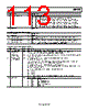
111 / 140 page  Data Sheet ADP1055 Rev. A | Page 111 of 140 Table 186. Register 0xFE49—PWM_DISABLE_SETTING Bits Bit Name R/W Description [7:6] Reserved R Reserved. 5 SR2 disable R/W Setting this bit disables the SR2 output. 4 SR1 disable R/W Setting this bit disables the SR1 output. 3 OUTD disable R/W Setting this bit disables the OUTD output. 2 OUTC disable R/W Setting this bit disables the OUTC output. 1 OUTB disable R/W Setting this bit disables the OUTB output. 0 OUTA disable R/W Setting this bit disables the OUTA output. Table 187. Register 0xFE4A—FILTER_TRANSITION (Requires Use of the GO Bit in Register 0xFE00) Bits Bit Name R/W Description 7 Overshoot protection R/W 0 = disable setpoint reference tracking. 1 = enable setpoint reference tracking (see the Integrator Windup and Output Voltage Regulation Loss (Overshoot Protection) section). 6 Overshoot speed R/W 0 = if VOUT is out of regulation for 96 out of 128 switching cycles, the reference moves to the last known value of VOUT (9-bit precision) and tries to return to regulation at a controlled rate given by the VOUT_TRANSITION_RATE command. 1 = if VOUT is out of regulation for 48 out of 64 switching cycles, VREF tracks VOUT (9-bit precision). Double update rate affects this register. [5:3] HF ADC configuration R/W 000 = autocorrection loop disabled. 001 = autocorrection loop bandwidth set to approximately 9 Hz. 010 = autocorrection loop bandwidth set to approximately 19 Hz. 011 = autocorrection loop bandwidth set to approximately 37 Hz. 100 = autocorrection loop bandwidth set to approximately 75 Hz. 101 = autocorrection loop bandwidth set to approximately 150 Hz. 110 = autocorrection loop bandwidth set to approximately 300 Hz. 111 = autocorrection loop bandwidth set to approximately 600 Hz. 2 Enable soft transition R/W Enables soft transition between filter settings to minimize output transients. All four parameters of each filter are linearly transitioned to the new value. [1:0] Transition speed R/W The filter changes in 32 steps, with one step applied at the interval specified by these bits. Bit 1 Bit 0 Speed 0 0 32 × tSW (total transition time = 32 × 32 × tSW = 1024 × tSW) 0 1 8 × tSW (total transition time = 8 × 32 = 256 × tSW) 1 0 2 × tSW (total = 64 × tSW) 1 1 1 × tSW (total = 32 × tSW) Table 188. Register 0xFE4B—DEEP_LLM_SETTING Bits Bit Name R/W Description [7:5] Deep LLM thresholds R/W These bits set the load current limit on the CS2 ADC below which SR1 and SR2 enter deep light load mode. The averaging time, debounce, and hysteresis are programmed in Register 0xFE4B. SR outputs are always off in pulse skip mode. Bit 7 Bit 6 Bit 5 Thresholds (LSBs) 0 0 0 0 0 0 1 4 0 1 0 8 0 1 1 12 1 0 0 16 1 0 1 20 1 1 0 24 1 1 1 28 |
|
ссылки URL |
| Вашему бизинису помогли Аллдатащит? [ DONATE ] |
Что такое Аллдатащит | реклама | контакт | Конфиденциальность | Ссылка на техническое описание | обмен ссыками | поиск по производителю All Rights Reserved©Alldatasheet.com |
| Russian : Alldatasheetru.com | Korean : Alldatasheet.co.kr | Spanish : Alldatasheet.es | French : Alldatasheet.fr | Italian : Alldatasheetit.com Portuguese : Alldatasheetpt.com | Polish : Alldatasheet.pl | Vietnamese : Alldatasheet.vn Indian : Alldatasheet.in | Mexican : Alldatasheet.com.mx | British : Alldatasheet.co.uk | New Zealand : Alldatasheet.co.nz |
|
Family Site : ic2ic.com |
icmetro.com |
 Russian ▼
 English
 Chinese
 German
 Japanese
 Russian
 Korean
 Spanish
 French
 Italian
 Portuguese
 Polish
 Vietnamese
 Indian
 Mexican
 British
 New Zealand