|
поискавой системы для электроныых деталей |
|
|
поискавой системы для электроныых деталей |
|
TMS320LC2401AVFS датащи(PDF) 12 Page - Texas Instruments |
|
|
|||||||||||||||||||||||||||||
TMS320LC2401AVFS датащи(HTML) 12 Page - Texas Instruments |
|
|
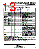
12 / 134 page  TMS320LF2407A,TMS320LF2406A,TMS320LF2403A,TMS320LF2402A TMS320LC2406A,TMS320LC2404A,TMS320LC2403A,TMS320LC2402A DSP CONTROLLERS SPRS145K − JULY 2000 − REVISED AUGUST 2005 12 POST OFFICE BOX 1443 • HOUSTON, TEXAS 77251−1443 pin functions (continued) Table 2. LF240xA and LC240xA Pin List and Package Options†‡ (Continued) PIN NAME LF2407A (144-PGE) 2406A (100-PZ) LC2404A (100-PZ) 2403A, LC2402A (64-PAG) and 2402A (64-PG) DESCRIPTION EVENT MANAGER B (EVB) (CONTINUED) T3PWM/T3CMP/IOPF2 8 7 7 Timer 3 compare output (EVB) or GPIO ( ↑) T4PWM/T4CMP/IOPF3 6 5 5 Timer 4 compare output (EVB) or GPIO ( ↑) TDIRB/IOPF4 2 2 2 Counting direction for general-purpose (GP) timer (EVB) or GPIO. If TDIRB = 1, upward counting is selected. If TDIRB = 0, downward counting is selected. ( ↑) TCLKINB/IOPF5 126 89 89 External clock input for GP timer (EVB) or GPIO. Note that the timer can also use the internal device clock. ( ↑) ANALOG-TO-DIGITAL CONVERTER (ADC) ADCIN00 112 79 79 18 Analog input #0 to the ADC ADCIN01 110 77 77 17 Analog input #1 to the ADC ADCIN02 107 74 74 16 Analog input #2 to the ADC ADCIN03 105 72 72 15 Analog input #3 to the ADC ADCIN04 103 70 70 14 Analog input #4 to the ADC ADCIN05 102 69 69 13 Analog input #5 to the ADC ADCIN06 100 67 67 12 Analog input #6 to the ADC ADCIN07 99 66 66 11 Analog input #7 to the ADC ADCIN08 113 80 80 Analog input #8 to the ADC ADCIN09 111 78 78 Analog input #9 to the ADC ADCIN10 109 76 76 Analog input #10 to the ADC ADCIN11 108 75 75 Analog input #11 to the ADC ADCIN12 106 73 73 Analog input #12 to the ADC ADCIN13 104 71 71 Analog input #13 to the ADC ADCIN14 101 68 68 Analog input #14 to the ADC ADCIN15 98 65 65 Analog input #15 to the ADC VREFHI 115 82 82 20 ADC analog high-voltage reference input VREFLO 114 81 81 19 ADC analog low-voltage reference input VCCA 116 83 83 21 Analog supply voltage for ADC (3.3 V)§ VSSA 117 84 84 22 Analog ground reference for ADC † Bold, italicized pin names indicate pin function after reset. ‡ GPIO − General-purpose input/output pin. All GPIOs come up as input after reset. § It is highly recommended that VCCA be isolated from the digital supply voltage (and VSSA from digital ground) to maintain the specified accuracy and improve the noise immunity of the ADC. ¶ Only when all of the following conditions are met: EMU1/OFF is low, TRST is low, and EMU0 is high # No power supply pin (VDD, VDDO, VSS, or VSSO) should be left unconnected. All power supply pins must be connected appropriately for proper device operation. LEGEND: ↑ − Internal pullup ↓ − Internal pulldown (Typical active pullup/pulldown value is ±16 µA.) |
|
ссылки URL |
| Вашему бизинису помогли Аллдатащит? [ DONATE ] |
Что такое Аллдатащит | реклама | контакт | Конфиденциальность | Ссылка на техническое описание | обмен ссыками | поиск по производителю All Rights Reserved©Alldatasheet.com |
| Russian : Alldatasheetru.com | Korean : Alldatasheet.co.kr | Spanish : Alldatasheet.es | French : Alldatasheet.fr | Italian : Alldatasheetit.com Portuguese : Alldatasheetpt.com | Polish : Alldatasheet.pl | Vietnamese : Alldatasheet.vn Indian : Alldatasheet.in | Mexican : Alldatasheet.com.mx | British : Alldatasheet.co.uk | New Zealand : Alldatasheet.co.nz |
|
Family Site : ic2ic.com |
icmetro.com |
 Russian ▼
 English
 Chinese
 German
 Japanese
 Russian
 Korean
 Spanish
 French
 Italian
 Portuguese
 Polish
 Vietnamese
 Indian
 Mexican
 British
 New Zealand