|
поискавой системы для электроныых деталей |
|
|
поискавой системы для электроныых деталей |
|
PIC16C71 датащи(PDF) 55 Page - Microchip Technology |
|
|
|||||||||||||||||||||||||||||
PIC16C71 датащи(HTML) 55 Page - Microchip Technology |
|
|
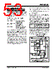
55 / 337 page  © 1997 Microchip Technology Inc. DS30234D-page 55 PIC16C6X 5.3 PORTC and TRISC Register PORTC is an 8-bit wide bi-directional port. Each pin is individually configurable as an input or output through the TRISC register. PORTC is multiplexed with several peripheral functions (Table 5-5). PORTC pins have Schmitt Trigger input buffers. When enabling peripheral functions, care should be taken in defining TRIS bits for each PORTC pin. Some peripherals override the TRIS bit to make a pin an out- put, while other peripherals override the TRIS bit to make a pin an input. Since the TRIS bit override is in effect while the peripheral is enabled, read-modify- write instructions (BSF, BCF, XORWF) with TRISC as destination should be avoided. The user should refer to the corresponding peripheral section for the correct TRIS bit settings. EXAMPLE 5-3: INITIALIZING PORTC BCF STATUS, RP0 ; BCF STATUS, RP1 ; PIC16C66/67 only CLRF PORTC ; Initialize PORTC by ; clearing output ; data latches BSF STATUS, RP0 ; Select Bank 1 MOVLW 0xCF ; Value used to ; initialize data ; direction MOVWF TRISC ; Set RC<3:0> as inputs ; RC<5:4> as outputs ; RC<7:6> as inputs Applicable Devices 61 62 62A R62 63 R63 64 64A R64 65 65A R65 66 67 FIGURE 5-6: PORTC BLOCK DIAGRAM PORT/PERIPHERAL Select(2) Data bus WR PORT WR TRIS RD Data Latch TRIS Latch RD TRIS Schmitt Trigger Q D Q CK QD EN Peripheral Data Out 0 1 Q D Q CK P N VDD VSS PORT Peripheral OE(3) Peripheral input I/O pin(1) Note 1: I/O pins have diode protection to VDD and VSS. 2: Port/Peripheral select signal selects between port data and peripheral output. 3: Peripheral OE (output enable) is only activated if peripheral select is active. TABLE 5-5: PORTC FUNCTIONS FOR PIC16C62/64 Name Bit# Buffer Type Function RC0/T1OSI/T1CKI bit0 ST Input/output port pin or Timer1 oscillator input or Timer1 clock input RC1/T1OSO bit1 ST Input/output port pin or Timer1 oscillator output RC2/CCP1 bit2 ST Input/output port pin or Capture1 input/Compare1 output/PWM1 output RC3/SCK/SCL bit3 ST RC3 can also be the synchronous serial clock for both SPI and I2C modes. RC4/SDI/SDA bit4 ST RC4 can also be the SPI Data In (SPI mode) or data I/O (I2C mode). RC5/SDO bit5 ST Input/output port pin or synchronous serial port data output RC6 bit6 ST Input/output port pin RC7 bit7 ST Input/output port pin Legend: ST = Schmitt Trigger input |
|
ссылки URL |
| Вашему бизинису помогли Аллдатащит? [ DONATE ] |
Что такое Аллдатащит | реклама | контакт | Конфиденциальность | Ссылка на техническое описание | обмен ссыками | поиск по производителю All Rights Reserved©Alldatasheet.com |
| Russian : Alldatasheetru.com | Korean : Alldatasheet.co.kr | Spanish : Alldatasheet.es | French : Alldatasheet.fr | Italian : Alldatasheetit.com Portuguese : Alldatasheetpt.com | Polish : Alldatasheet.pl | Vietnamese : Alldatasheet.vn Indian : Alldatasheet.in | Mexican : Alldatasheet.com.mx | British : Alldatasheet.co.uk | New Zealand : Alldatasheet.co.nz |
|
Family Site : ic2ic.com |
icmetro.com |
 Russian ▼
 English
 Chinese
 German
 Japanese
 Russian
 Korean
 Spanish
 French
 Italian
 Portuguese
 Polish
 Vietnamese
 Indian
 Mexican
 British
 New Zealand