 |
поискавой системы для электроныых деталей |
|
|
поискавой системы для электроныых деталей |
|
The question interval is too short.
Please try again in a few seconds.

Hello, Please ask a question about PIC16F684 Datasheet
# Example questions:
➢ What is the purpose of the pclath register?
➢ What determines whether bank 0 or bank 1 is selected for data access?
➢ What is the significance of the 'irp' and 'rp1' bits within the status register, according to the provided documentation?
| Part No. | PIC16F684 |
| Manufacturer | MICROCHIP |
| Size | 3Mb |
| Pages | 192 pages |
| Description | 14-Pin, Flash-Based 8-Bit CMOS Microcontrollers with nanoWatt Technology |












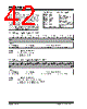
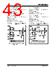
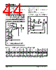
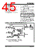















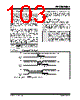
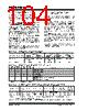
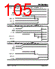


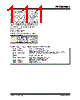







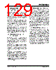


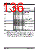


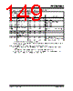
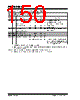
















What's Good:
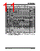
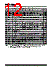
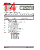
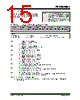
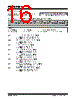
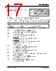
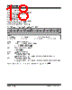
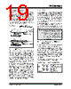
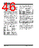
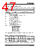
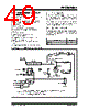
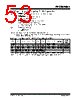
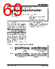
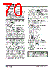
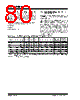
️· Structure: The layout is relatively clear. The division into Program Memory, Data Memory, and Special Function Registers (SFRs) is standard and helpful.
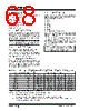
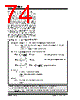
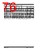
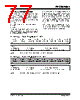
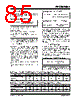
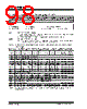
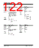
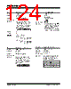
️· SFR Table: The table of SFRs is essential. It provides addresses, bit descriptions, and default values.
️· Bank Selection: Explaining the RP0 bit and bank selection is crucial.
️· Indirect Addressing: Briefly mentioning INDF and FSR is good; more details would be helpful (see suggestions below).
Areas for Improvement and Potential Expansions:
1. Figures:
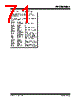
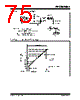
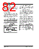
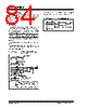
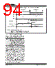
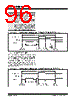
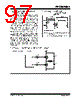
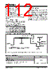
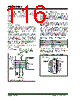
- Figure 2-1 (Program Memory Map): This is mentioned but not shown. Critical to include a diagram illustrating the program memory space, the reset vector, and the interrupt vector. This helps visualize program execution.
- Figure 2-2 (Data Memory Map): This is also mentioned but not included. A visual representation of the data memory organization, clearly showing Banks 0 and 1, GPRs, SFRs, and the addressing scheme is essential.
2. Indirect Addressing (INDF & FSR) - Expansion Needed:
- The brief mention of INDF and FSR is a setup, but more detail is necessary. Explain:
■ How FSR holds the address of the data memory location.
■ How INDF (Indirect FSR) automatically uses the value in FSR to access the data at the specified address. (INDF isn't a physical register, it’s a way to access data indirectly).
■ A simple code example of using INDF and FSR would clarify this concept. (e.g., `MOVLW 0x10; FSR = 0x10; INDF = 0x10; //Data at location 0x10 is now 0x10`)
3. SFR Table Improvements:
- Page References: The "Page" column is good for directing the reader to more detailed descriptions of the SFRs, but the page numbers should be verified and accurate.
- Bit Descriptions: While the table lists what each bit *is*, a brief explanation of its *function* would be incredibly helpful. For example, for `STATUS`:
■ `Z`: Zero bit – Set if the last arithmetic operation resulted in zero.
■ `DC`: Decimal mode bit – Enables/disables BCD arithmetic.
■ `C`: Carry bit – Set if the last arithmetic operation resulted in a carry-out.
- Default Values: Explicitly state the default value on Power-on Reset (POR) and Brown-out Reset (BOR) for each SFR.
- Unimplemented Bits/Registers: For unimplemented bits or registers, explicitly state that they are unimplemented, and reading them will return zero. This prevents misinterpretation.
4. Data Memory Banks:
- Explain how the bank selection affects the addressing of GPRs and SFRs.
5. Program Counter (PC):
- Expand a little on how PC operates.
6. Interrupt Vectors:
- Expand on the interrupt vectors and what interrupts are available.
7. Legend: The provided legend is good, but consider adding a description of what POR and BOR signify.
Example of Enhanced SFR Table Snippet (STATUS Register):
| Address | Name | Bit 2:0 | Bit 3 | Bit 4 | Bit 3 | Bit 1 | Bit 0 | Value on POR/BOR | Page | ||
|---|---|---|---|---|---|---|---|---|---|---|---|
| 03h | STATUS | IRP | RP1 | RP0 | TO | PD | Z | DC | C | ||
| 0001 1xxx | 13,104 | ||||||||||
| Description | |||||||||||
| IRP | Interrupt Request Priority | ||||||||||
| RP1, RP0 | Register Bank Select (Bits) | ||||||||||
| TO | Timer 0 Overflow Bit | ||||||||||
| PD | Power-down Bit | ||||||||||
| Z | Zero Bit | ||||||||||
| DC | Decimal Mode Bit | ||||||||||
| C | Carry Bit |
What's Good:
️· Structure: The layout is relatively clear. The division into Program Memory, Data Memory, and Special Function Registers (SFRs) is standard and helpful.
️· SFR Table: The table of SFRs is essential. It provides addresses, bit descriptions, and default values.
️· Bank Selection: Explaining the RP0 bit and bank selection is crucial.
️· Indirect Addressing: Briefly mentioning INDF and FSR is good; more details would be helpful (see suggestions below).
Areas for Improvement and Potential Expansions:
1. Figures:
- Figure 2-1 (Program Memory Map): This is mentioned but not shown. Critical to include a diagram illustrating the program memory space, the reset vector, and the interrupt vector. This helps visualize program execution.
- Figure 2-2 (Data Memory Map): This is also mentioned but not included. A visual representation of the data memory organization, clearly showing Banks 0 and 1, GPRs, SFRs, and the addressing scheme is essential.
2. Indirect Addressing (INDF & FSR) - Expansion Needed:
- The brief mention of INDF and FSR is a setup, but more detail is necessary. Explain:
■ How FSR holds the address of the data memory location.
■ How INDF (Indirect FSR) automatically uses the value in FSR to access the data at the specified address. (INDF isn't a physical register, it’s a way to access data indirectly).
■ A simple code example of using INDF and FSR would clarify this concept. (e.g., `MOVLW 0x10; FSR = 0x10; INDF = 0x10; //Data at location 0x10 is now 0x10`)
3. SFR Table Improvements:
- Page References: The "Page" column is good for directing the reader to more detailed descriptions of the SFRs, but the page numbers should be verified and accurate.
- Bit Descriptions: While the table lists what each bit *is*, a brief explanation of its *function* would be incredibly helpful. For example, for `STATUS`:
■ `Z`: Zero bit – Set if the last arithmetic operation resulted in zero.
■ `DC`: Decimal mode bit – Enables/disables BCD arithmetic.
■ `C`: Carry bit – Set if the last arithmetic operation resulted in a carry-out.
- Default Values: Explicitly state the default value on Power-on Reset (POR) and Brown-out Reset (BOR) for each SFR.
- Unimplemented Bits/Registers: For unimplemented bits or registers, explicitly state that they are unimplemented, and reading them will return zero. This prevents misinterpretation.
4. Data Memory Banks:
- Explain how the bank selection affects the addressing of GPRs and SFRs.
5. Program Counter (PC):
- Expand a little on how PC operates.
6. Interrupt Vectors:
- Expand on the interrupt vectors and what interrupts are available.
7. Legend: The provided legend is good, but consider adding a description of what POR and BOR signify.
Example of Enhanced SFR Table Snippet (STATUS Register):
| Address | Name | Bit 2:0 | Bit 3 | Bit 4 | Bit 3 | Bit 1 | Bit 0 | Value on POR/BOR | Page | ||
|---|---|---|---|---|---|---|---|---|---|---|---|
| 03h | STATUS | IRP | RP1 | RP0 | TO | PD | Z | DC | C | ||
| 0001 1xxx | 13,104 | ||||||||||
| Description | |||||||||||
| IRP | Interrupt Request Priority | ||||||||||
| RP1, RP0 | Register Bank Select (Bits) | ||||||||||
| TO | Timer 0 Overflow Bit | ||||||||||
| PD | Power-down Bit | ||||||||||
| Z | Zero Bit | ||||||||||
| DC | Decimal Mode Bit | ||||||||||
| C | Carry Bit |
| Part No. | PIC16F684 |
| Manufacturer | MICROCHIP |
| Size | 3Mb |
| Pages | 192 pages |
| Description | 14-Pin, Flash-Based 8-Bit CMOS Microcontrollers with nanoWatt Technology |
| Вашему бизинису помогли Аллдатащит? [ DONATE ] |
Что такое Аллдатащит | реклама | контакт | Конфиденциальность | Ссылка на техническое описание | обмен ссыками | поиск по производителю All Rights Reserved©Alldatasheet.com |
| Russian : Alldatasheetru.com | Korean : Alldatasheet.co.kr | Spanish : Alldatasheet.es | French : Alldatasheet.fr | Italian : Alldatasheetit.com Portuguese : Alldatasheetpt.com | Polish : Alldatasheet.pl | Vietnamese : Alldatasheet.vn Indian : Alldatasheet.in | Mexican : Alldatasheet.com.mx | British : Alldatasheet.co.uk | New Zealand : Alldatasheet.co.nz |
|
Family Site : ic2ic.com |
icmetro.com |
 Russian ▼
  English
 Chinese
 German
 Japanese
 Korean
 Spanish
 French
 Italian
 Portuguese
 Polish
 Vietnamese
 Indian
 Mexican
 British
 New Zealand