|
поискавой системы для электроныых деталей |
|
|
поискавой системы для электроныых деталей |
|
PIC16F684 датащи(PDF) 12 Page - Microchip Technology |
|
|
|||||||||||||||||||||||||||||
PIC16F684 датащи(HTML) 12 Page - Microchip Technology |
|
|
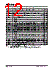
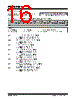
12 / 192 page  PIC16F684 DS41202F-page 10 © 2007 Microchip Technology Inc. TABLE 2-2: PIC16F684 SPECIAL FUNCTION REGISTERS SUMMARY BANK 1 Addr Name Bit 7 Bit 6 Bit 5 Bit 4 Bit 3 Bit 2 Bit 1 Bit 0 Value on POR, BOR Page Bank 1 80h INDF Addressing this location uses contents of FSR to address data memory (not a physical register) xxxx xxxx 19, 104 81h OPTION_REG RAPU INTEDG T0CS T0SE PSA PS2 PS1 PS0 1111 1111 14, 104 82h PCL Program Counter’s (PC) Least Significant Byte 0000 0000 19, 104 83h STATUS IRP(1) RP1(1) RP0 TO PD ZDC C 0001 1xxx 13, 104 84h FSR Indirect Data Memory Address Pointer xxxx xxxx 19, 104 85h TRISA — — TRISA5 TRISA4 TRISA3 TRISA2 TRISA1 TRISA0 --11 1111 31, 104 86h — Unimplemented — — 87h TRISC — — TRISC5 TRISC4 TRISC3 TRISC2 TRISC1 TRISC0 --11 1111 40, 104 88h — Unimplemented — — 89h — Unimplemented — — 8Ah PCLATH — — — Write Buffer for upper 5 bits of Program Counter ---0 0000 19, 104 8Bh INTCON GIE PEIE T0IE INTE RAIE T0IF INTF RAIF 0000 0000 15, 104 8Ch PIE1 EEIE ADIE CCP1IE C2IE C1IE OSFIE TMR2IE TMR1IE 0000 0000 16, 104 8Dh — Unimplemented — — 8Eh PCON — — ULPWUE SBOREN — —POR BOR --01 --qq 18, 104 8Fh OSCCON — IRCF2 IRCF1 IRCF0 OSTS(2) HTS LTS SCS -110 x000 20, 104 90h OSCTUNE — — — TUN4 TUN3 TUN2 TUN1 TUN0 ---0 0000 24, 105 91h ANSEL ANS7 ANS6 ANS5 ANS4 ANS3 ANS2 ANS1 ANS0 1111 1111 32, 105 92h PR2 Timer2 Module Period Register 1111 1111 53, 105 93h — Unimplemented — — 94h — Unimplemented — — 95h WPUA(3) — — WPUA5 WPUA4 — WPUA2 WPUA1 WPUA0 --11 -111 33, 105 96h IOCA — — IOCA5 IOCA4 IOCA3 IOCA2 IOCA1 IOCA0 --00 0000 33, 105 97h — Unimplemented — — 98h — Unimplemented — — 99h VRCON VREN —VRR — VR3 VR2 VR1 VR0 0-0- 0000 63, 105 9Ah EEDAT EEDAT7 EEDAT6 EEDAT5 EEDAT4 EEDAT3 EEDAT2 EEDAT1 EEDAT0 0000 0000 75, 105 9Bh EEADR EEADR7 EEADR6 EEADR5 EEADR4 EEADR3 EEADR2 EEADR1 EEADR0 0000 0000 75, 105 9Ch EECON1 — — — — WRERR WREN WR RD ---- x000 76, 105 9Dh EECON2 EEPROM Control Register 2 (not a physical register) ---- ---- 76, 105 9Eh ADRESL Least Significant 2 bits of the left shifted result or 8 bits of the right shifted result xxxx xxxx 71, 105 9Fh ADCON1 — ADCS2 ADCS1 ADCS0 — — — — -000 ---- 70, 105 Legend: – = Unimplemented locations read as ‘0’, u = unchanged, x = unknown, q = value depends on condition, shaded = unimplemented Note 1: IRP and RP1 bits are reserved, always maintain these bits clear. 2: OSTS bit of the OSCCON register reset to ‘0’ with Dual Speed Start-up and LP, HS or XT selected as the oscillator. 3: RA3 pull-up is enabled when MCLRE is ‘1’ in the Configuration Word register. |
|
ссылки URL |
| Вашему бизинису помогли Аллдатащит? [ DONATE ] |
Что такое Аллдатащит | реклама | контакт | Конфиденциальность | Ссылка на техническое описание | обмен ссыками | поиск по производителю All Rights Reserved©Alldatasheet.com |
| Russian : Alldatasheetru.com | Korean : Alldatasheet.co.kr | Spanish : Alldatasheet.es | French : Alldatasheet.fr | Italian : Alldatasheetit.com Portuguese : Alldatasheetpt.com | Polish : Alldatasheet.pl | Vietnamese : Alldatasheet.vn Indian : Alldatasheet.in | Mexican : Alldatasheet.com.mx | British : Alldatasheet.co.uk | New Zealand : Alldatasheet.co.nz |
|
Family Site : ic2ic.com |
icmetro.com |
 Russian ▼
 English
 Chinese
 German
 Japanese
 Russian
 Korean
 Spanish
 French
 Italian
 Portuguese
 Polish
 Vietnamese
 Indian
 Mexican
 British
 New Zealand