|
поискавой системы для электроныых деталей |
|
|
поискавой системы для электроныых деталей |
|
PIC16F684 датащи(PDF) 98 Page - Microchip Technology |
|
|
|||||||||||||||||||||||||||||
PIC16F684 датащи(HTML) 98 Page - Microchip Technology |
|
|
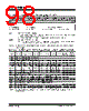
98 / 192 page  PIC16F684 DS41202F-page 96 © 2007 Microchip Technology Inc. TABLE 11-5: SUMMARY OF REGISTERS ASSOCIATED WITH CAPTURE, COMPARE AND PWM REGISTER 11-3: PWM1CON: ENHANCED PWM CONTROL REGISTER R/W-0 R/W-0 R/W-0 R/W-0 R/W-0 R/W-0 R/W-0 R/W-0 PRSEN PDC6 PDC5 PDC4 PDC3 PDC2 PDC1 PDC0 bit 7 bit 0 Legend: R = Readable bit W = Writable bit U = Unimplemented bit, read as ‘0’ -n = Value at POR ‘1’ = Bit is set ‘0’ = Bit is cleared x = Bit is unknown bit 7 PRSEN: PWM Restart Enable bit 1 = Upon auto-shutdown, the ECCPASE bit clears automatically once the shutdown event goes away; the PWM restarts automatically 0 = Upon auto-shutdown, ECCPASE must be cleared in software to restart the PWM bit 6-0 PDC<6:0>: PWM Delay Count bits PDCn = Number of FOSC/4 (4 * TOSC) cycles between the scheduled time when a PWM signal should transition active and the actual time it transitions active Note 1: Bit resets to ‘0’ with Two-Speed Start-up and LP, XT or HS selected as the Oscillator mode or Fail-Safe mode is enabled. Name Bit 7 Bit 6 Bit 5 Bit 4 Bit 3 Bit 2 Bit 1 Bit 0 Value on: POR, BOR Value on all other Resets CCPR1L Capture/Compare/PWM Register 1 Low Byte xxxx xxxx uuuu uuuu CCPR1H Capture/Compare/PWM Register 1 High Byte xxxx xxxx uuuu uuuu CCP1CON P1M1 P1M0 DC1B1 DC1B0 CCP1M3 CCP1M2 CCP1M1 CCP1M0 0000 0000 0000 0000 CMCON0 C2OUT C1OUT C2INV C1INV CIS CM2 CM1 CM0 0000 0000 0000 0000 CMCON1 — — — — — — T1GSS C2SYNC ---- --10 ---- --10 ECCPAS ECCPASE ECCPAS2 ECCPAS1 ECCPAS0 PSSAC1 PSSAC0 PSSBD1 PSSBD0 0000 0000 0000 0000 INTCON GIE PEIE T0IE INTE RAIE T0IF INTF RAIF 0000 0000 0000 0000 PIE1 EEIE ADIE CCP1IE C2IE C1IE OSFIE TMR2IE TMR1IE 0000 0000 0000 0000 PIR1 EEIF ADIF CCP1IF C2IF C1IF OSFIF TMR2IF TMR1IF 0000 0000 0000 0000 PR2 Timer2 Module Period Register 1111 1111 1111 1111 PWM1CON PRSEN PDC6 PDC5 PDC4 PDC3 PDC2 PDC1 PDC0 0000 0000 0000 0000 T1CON T1GINV TMR1GE T1CKPS1 T1CKPS0 T1OSCEN T1SYNC TMR1CS TMR1ON 0000 0000 uuuu uuuu T2CON — TOUTPS3 TOUTPS2 TOUTPS1 TOUTPS0 TMR2ON T2CKPS1 T2CKPS0 -000 0000 -000 0000 TMR1L Holding Register for the Least Significant Byte of the 16-bit TMR1 Register xxxx xxxx uuuu uuuu TMR1H Holding Register for the Most Significant Byte of the 16-bit TMR1 Register xxxx xxxx uuuu uuuu TMR2 Timer2 Module Register 0000 0000 0000 0000 TRISA — — TRISA5 TRISA4 TRISA3 TRISA2 TRISA1 TRISA0 --11 1111 --11 1111 TRISC — — TRISC5 TRISC4 TRISC3 TRISC2 TRISC1 TRISC0 --11 1111 --11 1111 Legend: - = Unimplemented locations, read as ‘0’, u = unchanged, x = unknown. Shaded cells are not used by the Capture, Compare and PWM. |
|
ссылки URL |
| Вашему бизинису помогли Аллдатащит? [ DONATE ] |
Что такое Аллдатащит | реклама | контакт | Конфиденциальность | Ссылка на техническое описание | обмен ссыками | поиск по производителю All Rights Reserved©Alldatasheet.com |
| Russian : Alldatasheetru.com | Korean : Alldatasheet.co.kr | Spanish : Alldatasheet.es | French : Alldatasheet.fr | Italian : Alldatasheetit.com Portuguese : Alldatasheetpt.com | Polish : Alldatasheet.pl | Vietnamese : Alldatasheet.vn Indian : Alldatasheet.in | Mexican : Alldatasheet.com.mx | British : Alldatasheet.co.uk | New Zealand : Alldatasheet.co.nz |
|
Family Site : ic2ic.com |
icmetro.com |
 Russian ▼
 English
 Chinese
 German
 Japanese
 Russian
 Korean
 Spanish
 French
 Italian
 Portuguese
 Polish
 Vietnamese
 Indian
 Mexican
 British
 New Zealand