|
поискавой системы для электроныых деталей |
|
|
поискавой системы для электроныых деталей |
|
PIC16F684 датащи(PDF) 61 Page - Microchip Technology |
|
|
|||||||||||||||||||||||||||||
PIC16F684 датащи(HTML) 61 Page - Microchip Technology |
|
|
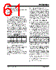
61 / 192 page  © 2007 Microchip Technology Inc. DS41202F-page 59 PIC16F684 8.3 Comparator Control The CMCON0 register (Register 8-1) provides access to the following comparator features: • Mode selection • Output state • Output polarity • Input switch 8.3.1 COMPARATOR OUTPUT STATE Each comparator state can always be read internally via the associated CxOUT bit of the CMCON0 register. The comparator outputs are directed to the CxOUT pins when CM<2:0> = 110. When this mode is selected, the TRIS bits for the associated CxOUT pins must be cleared to enable the output drivers. 8.3.2 COMPARATOR OUTPUT POLARITY Inverting the output of a comparator is functionally equivalent to swapping the comparator inputs. The polarity of a comparator output can be inverted by set- ting the CxINV bits of the CMCON0 register. Clearing CxINV results in a non-inverted output. A complete table showing the output state versus input conditions and the polarity bit is shown in Table 8-1. TABLE 8-1: OUTPUT STATE VS. INPUT CONDITIONS 8.3.3 COMPARATOR INPUT SWITCH The inverting input of the comparators may be switched between two analog pins in the following modes: • CM<2:0> = 001 (Comparator C1 only) • CM<2:0> = 010 (Comparators C1 and C2) In the above modes, both pins remain in Analog mode regardless of which pin is selected as the input. The CIS bit of the CMCON0 register controls the comparator input switch. 8.4 Comparator Response Time The comparator output is indeterminate for a period of time after the change of an input source or the selection of a new reference voltage. This period is referred to as the response time. The response time of the comparator differs from the settling time of the voltage reference. Therefore, both of these times must be considered when determining the total response time to a comparator input change. See Comparator and Voltage Reference specifications of Section 15.0 “Electrical Specifications” for more details. 8.5 Comparator Interrupt Operation The comparator interrupt flag is set whenever there is a change in the output value of the comparator. Changes are recognized by means of a mismatch circuit which consists of two latches and an exclusive- or gate (see Figure 8-2 and Figure 8-3). One latch is updated with the comparator output level when the CMCON0 register is read. This latch retains the value until the next read of the CMCON0 register or the occurrence of a reset. The other latch of the mismatch circuit is updated on every Q1 system clock. A mismatch condition will occur when a comparator output change is clocked through the second latch on the Q1 clock cycle. The mismatch condition will persist, holding the CxIF bit of the PIR1 register true, until either the CMCON0 register is read or the comparator output returns to the previous state. Software will need to maintain information about the status of the comparator output to determine the actual change that has occurred. The CxIF bit of the PIR1 register is the comparator interrupt flag. This bit must be reset in software by clearing it to ‘0’. Since it is also possible to write a ‘1’ to this register, a simulated interrupt may be initiated. The CxIE bit of the PIE1 register and the PEIE and GIE bits of the INTCON register must all be set to enable comparator interrupts. If any of these bits are cleared, the interrupt is not enabled, although the CxIF bit of the PIR1 register will still be set if an interrupt condition occurs. The user, in the Interrupt Service Routine, can clear the interrupt in the following manner: a) Any read or write of CMCON0. This will end the mismatch condition. b) Clear the CxIF interrupt flag. Input Conditions CxINV CxOUT VIN- > VIN+ 00 VIN- < VIN+ 01 VIN- > VIN+ 11 VIN- < VIN+ 10 Note: CxOUT refers to both the register bit and output pin. Note: A write operation to the CMCON0 register will also clear the mismatch condition because all writes include a read operation at the beginning of the write cycle. |
|
ссылки URL |
| Вашему бизинису помогли Аллдатащит? [ DONATE ] |
Что такое Аллдатащит | реклама | контакт | Конфиденциальность | Ссылка на техническое описание | обмен ссыками | поиск по производителю All Rights Reserved©Alldatasheet.com |
| Russian : Alldatasheetru.com | Korean : Alldatasheet.co.kr | Spanish : Alldatasheet.es | French : Alldatasheet.fr | Italian : Alldatasheetit.com Portuguese : Alldatasheetpt.com | Polish : Alldatasheet.pl | Vietnamese : Alldatasheet.vn Indian : Alldatasheet.in | Mexican : Alldatasheet.com.mx | British : Alldatasheet.co.uk | New Zealand : Alldatasheet.co.nz |
|
Family Site : ic2ic.com |
icmetro.com |
 Russian ▼
 English
 Chinese
 German
 Japanese
 Russian
 Korean
 Spanish
 French
 Italian
 Portuguese
 Polish
 Vietnamese
 Indian
 Mexican
 British
 New Zealand