|
поискавой системы для электроныых деталей |
|
|
поискавой системы для электроныых деталей |
|
PCA5010 датащи(PDF) 21 Page - NXP Semiconductors |
|
|
|||||||||||||||||||||||||||||
PCA5010 датащи(HTML) 21 Page - NXP Semiconductors |
|
|
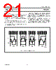
21 / 112 page  1998 Nov 02 21 Philips Semiconductors Product specification Pager baseband controller PCA5010 6.8.2 TIMING The timing of the I2C-bus interface is based on the internal 6 MHz clock. The phases of this clock divided-by-4 are used as a reference in the 400 kHz mode and divided-by-16 in the 100 kHz mode. In the following context ‘T’ (333 ns or 1.33 µs) denotes a single phase of this clock. The transfer of a single bit lasts 9 T. SCL is HIGH for 5 T. When receiving data, the PCA5010 samples the SDA line after 3 T while SCL is HIGH. The implemented I2C-bus Interface operates according to the timing diagram in Fig.9. The open-drain I2C-bus outputs are implemented as slew rate controlled driver stages, to minimize the negative impact of I2C-bus activity on the pager sensitivity while the pager is receiving. Typical waveforms on P1.7 (SDA) and P1.6 (SCL) are shown in Fig.10. Because SDA and SCL are open-drain type I/Os, only the falling edge is determined by the driver characteristics. The static sink current when driving LOW and the slope of the rising edges are determined by the capacitive I2C-bus load and its resistive termination (pull-up to VDD). Fig.9 Timing of the I2C-bus interface. handbook, full pagewidth MGR337 3T 4T START SCL SDA STOP 5T 2T 2T 2T TX bit 2T 2T 5T 2T 2T 3T 2T RX bit |
|
ссылки URL |
| Вашему бизинису помогли Аллдатащит? [ DONATE ] |
Что такое Аллдатащит | реклама | контакт | Конфиденциальность | Ссылка на техническое описание | обмен ссыками | поиск по производителю All Rights Reserved©Alldatasheet.com |
| Russian : Alldatasheetru.com | Korean : Alldatasheet.co.kr | Spanish : Alldatasheet.es | French : Alldatasheet.fr | Italian : Alldatasheetit.com Portuguese : Alldatasheetpt.com | Polish : Alldatasheet.pl | Vietnamese : Alldatasheet.vn Indian : Alldatasheet.in | Mexican : Alldatasheet.com.mx | British : Alldatasheet.co.uk | New Zealand : Alldatasheet.co.nz |
|
Family Site : ic2ic.com |
icmetro.com |
 Russian ▼
 English
 Chinese
 German
 Japanese
 Russian
 Korean
 Spanish
 French
 Italian
 Portuguese
 Polish
 Vietnamese
 Indian
 Mexican
 British
 New Zealand