|
поискавой системы для электроныых деталей |
|
|
поискавой системы для электроныых деталей |
|
PCA5010 датащи(PDF) 84 Page - NXP Semiconductors |
|
|
|||||||||||||||||||||||||||||
PCA5010 датащи(HTML) 84 Page - NXP Semiconductors |
|
|
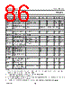
84 / 112 page  1998 Nov 02 84 Philips Semiconductors Product specification Pager baseband controller PCA5010 Notes 1. DC/DC converter configured with inductor of L = 470 µH, SRL = 5 Ω, input capacitance of Ci = 4.7 µF, ESR = 0.5 Ω, VDD output capacitor Co = 4.7 µF, ESR = 0.5 Ω, RBAT <1 Ω. 2. The required VBAT for starting the circuit after connecting it to the battery is 1.1 V. But once in place, the battery can be used until it is discharged to 0.9 V. 3. This parameter is not tested during production; it is guaranteed by design. 4. This parameter is not tested during production; it is covered by other measurements. 5. The accuracy of the voltage is defined by maximum offset and ripple voltage. DC offset is defined by the accuracy of the internal band gap reference and the offset of comparators, whereas the ripple voltage is defined by the limits of the allowed voltage window of the regulated VDD. 6. The ripple in standby mode is defined by VBAT, L, tn and ESR (see Table 54). 7. PCA5010 set to standby mode by software: 76.8 kHz oscillator running, DC/DC converter running in standby mode, all timer/counters disabled except RTC, microcontroller Idle, all outputs open-circuit, no IDD delivered to external circuits. 8. This parameter depends on external components and is not tested during production; hence no guarantee. 9. Rs = total series resistance = RBAT +SRL+RDS(on) + ESR. 10. PCA5010 set to receive mode by software: 76.8 kHz and 6 MHz oscillator running, DC/DC converter running in normal mode, wake-up counter, clock compensation, watchdog timer, T0 and T1 enabled, demodulator set to direct input data, AFC disabled, microcontroller Idle, all outputs open-circuit, no IDD delivered to external circuits. 11. The minimum supply voltage is determined by the start-up sequence of the device. When the start-up sequence is completed, the supply voltage can be lowered to 1.8 V. 12. The microcontroller operates with approximately 1.9 million instructions per second at a VDD = 2.2 V. The current consumption at this VDD is 0.7 mA/MIPS (peripheral blocks as e.g. timers, DC/DC converter, I2C-bus, UART, demodulator etc., are excluded). The current required from VDD is then 1.35 mA (typ.). This scales to sunk from VBAT. 13. In mass program mode the current can increase to 100 mA. CL(DAC) allowed capacitive load at DAC output −− 50 pF Isource(DAC) AFCOUT source current VDD = 2.2 V; VAFCOUT =VDD − 0.4 V; code = 111111 −−895 −100 µA Isink(DAC) AFCOUT sink current VDD = 2.2 V; VAFCOUT = 0.4 V; code = 000000 10 25 −µA SYMBOL PARAMETER CONDITIONS MIN. TYP. MAX. UNIT I BAT V DD V BAT ------------ I DD × 2.5 mA == |
|
ссылки URL |
| Вашему бизинису помогли Аллдатащит? [ DONATE ] |
Что такое Аллдатащит | реклама | контакт | Конфиденциальность | Ссылка на техническое описание | обмен ссыками | поиск по производителю All Rights Reserved©Alldatasheet.com |
| Russian : Alldatasheetru.com | Korean : Alldatasheet.co.kr | Spanish : Alldatasheet.es | French : Alldatasheet.fr | Italian : Alldatasheetit.com Portuguese : Alldatasheetpt.com | Polish : Alldatasheet.pl | Vietnamese : Alldatasheet.vn Indian : Alldatasheet.in | Mexican : Alldatasheet.com.mx | British : Alldatasheet.co.uk | New Zealand : Alldatasheet.co.nz |
|
Family Site : ic2ic.com |
icmetro.com |
 Russian ▼
 English
 Chinese
 German
 Japanese
 Russian
 Korean
 Spanish
 French
 Italian
 Portuguese
 Polish
 Vietnamese
 Indian
 Mexican
 British
 New Zealand