|
поискавой системы для электроныых деталей |
|
|
поискавой системы для электроныых деталей |
|
PIC16F627A датащи(PDF) 93 Page - Microchip Technology |
|
|
|||||||||||||||||||||||||||||
PIC16F627A датащи(HTML) 93 Page - Microchip Technology |
|
|
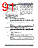
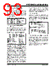
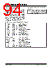
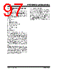
93 / 180 page  © 2005 Microchip Technology Inc. DS40044D-page 91 PIC16F627A/628A/648A 13.3 Reading the EEPROM Data Memory To read a data memory location, the user must write the address to the EEADR register and then set control bit RD (EECON1<0>). The data is available, in the very next cycle, in the EEDATA register; therefore it can be read in the next instruction. EEDATA will hold this value until another read or until it is written to by the user (during a write operation). EXAMPLE 13-1: DATA EEPROM READ 13.4 Writing to the EEPROM Data Memory To write an EEPROM data location, the user must first write the address to the EEADR register and the data to the EEDATA register. Then the user must follow a specific sequence to initiate the write for each byte. EXAMPLE 13-2: DATA EEPROM WRITE The write will not initiate if the above sequence is not followed exactly (write 55h to EECON2, write AAh to EECON2, then set WR bit) for each byte. We strongly recommend that interrupts be disabled during this code segment. A cycle count is executed during the required sequence. Any number that is not equal to the required cycles to execute the required sequence will cause the data not to be written into the EEPROM. Additionally, the WREN bit in EECON1 must be set to enable write. This mechanism prevents accidental writes to data EEPROM due to errant (unexpected) code execution (i.e., lost programs). The user should keep the WREN bit clear at all times, except when updating EEPROM. The WREN bit is not cleared by hardware. After a write sequence has been initiated, clearing the WREN bit will not affect this write cycle. The WR bit will be inhibited from being set unless the WREN bit is set. At the completion of the write cycle, the WR bit is cleared in hardware and the EE Write Complete Interrupt Flag bit (EEIF) is set. The user can either enable this interrupt or poll this bit. The EEIF bit in the PIR1 registers must be cleared by software. 13.5 Write Verify Depending on the application, good programming practice may dictate that the value written to the Data EEPROM should be verified (Example 13-3) to the desired value to be written. This should be used in applications where an EEPROM bit will be stressed near the specification limit. EXAMPLE 13-3: WRITE VERIFY 13.6 Protection Against Spurious Write There are conditions when the device may not want to write to the data EEPROM memory. To protect against spurious EEPROM writes, various mechanisms have been built-in. On power-up, WREN is cleared. Also when enabled, the Power-up Timer (72 ms duration) prevents EEPROM write. The write initiate sequence and the WREN bit together help prevent an accidental write during brown-out, power glitch or software malfunction. BSF STATUS, RP0 ;Bank 1 MOVLW CONFIG_ADDR ; MOVWF EEADR ;Address to read BSF EECON1, RD ;EE Read MOVF EEDATA, W ;W = EEDATA BCF STATUS, RP0 ;Bank 0 BSF STATUS, RP0 ;Bank 1 BSF EECON1, WREN ;Enable write BCF INTCON, GIE ;Disable INTs. BTFSC INTCON,GIE ;See AN576 GOTO $-2 MOVLW 55h ; MOVWF EECON2 ;Write 55h MOVLW AAh ; MOVWF EECON2 ;Write AAh BSF EECON1,WR ;Set WR bit ;begin write BSF INTCON, GIE ;Enable INTs. BSF STATUS, RP0 ;Bank 1 MOVF EEDATA, W BSF EECON1, RD ;Read the ;value written ; ;Is the value written (in W reg) and ;read (in EEDATA) the same? ; SUBWF EEDATA, W ; BTFSS STATUS, Z ;Is difference 0? GOTO WRITE_ERR ;NO, Write error : ;YES, Good write : ;Continue program |
|
ссылки URL |
| Вашему бизинису помогли Аллдатащит? [ DONATE ] |
Что такое Аллдатащит | реклама | контакт | Конфиденциальность | Ссылка на техническое описание | обмен ссыками | поиск по производителю All Rights Reserved©Alldatasheet.com |
| Russian : Alldatasheetru.com | Korean : Alldatasheet.co.kr | Spanish : Alldatasheet.es | French : Alldatasheet.fr | Italian : Alldatasheetit.com Portuguese : Alldatasheetpt.com | Polish : Alldatasheet.pl | Vietnamese : Alldatasheet.vn Indian : Alldatasheet.in | Mexican : Alldatasheet.com.mx | British : Alldatasheet.co.uk | New Zealand : Alldatasheet.co.nz |
|
Family Site : ic2ic.com |
icmetro.com |
 Russian ▼
 English
 Chinese
 German
 Japanese
 Russian
 Korean
 Spanish
 French
 Italian
 Portuguese
 Polish
 Vietnamese
 Indian
 Mexican
 British
 New Zealand