|
поискавой системы для электроныых деталей |
|
|
поискавой системы для электроныых деталей |
|
PIC16F627A датащи(PDF) 61 Page - Microchip Technology |
|
|
|||||||||||||||||||||||||||||
PIC16F627A датащи(HTML) 61 Page - Microchip Technology |
|
|
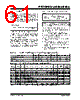
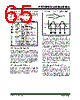
61 / 180 page  © 2005 Microchip Technology Inc. DS40044D-page 59 PIC16F627A/628A/648A 9.3.2 PWM DUTY CYCLE The PWM duty cycle is specified by writing to the CCPR1L register and to the CCP1CON<5:4> bits. Up to 10-bit resolution is available: the CCPR1L contains the eight MSbs and the CCP1CON<5:4> contains the two LSbs. This 10-bit value is represented by CCPR1L:CCP1CON<5:4>. The following equation is used to calculate the PWM duty cycle in time: CCPR1L and CCP1CON<5:4> can be written to at any time, but the duty cycle value is not latched into CCPR1H until after a match between PR2 and TMR2 occurs (i.e., the period is complete). In PWM mode, CCPR1H is a read-only register. The CCPR1H register and a 2-bit internal latch are used to double buffer the PWM duty cycle. This double buffering is essential for glitchless PWM operation. When the CCPR1H and 2-bit latch match TMR2 concatenated with an internal 2-bit Q clock or 2 bits of the TMR2 prescaler, the CCP1 pin is cleared. Maximum PWM resolution (bits) for a given PWM frequency: For an example PWM period and duty cycle calculation, see the PICmicro® Mid-Range Reference Manual (DS33023). 9.3.3 SET-UP FOR PWM OPERATION The following steps should be taken when configuring the CCP module for PWM operation: 1. Set the PWM period by writing to the PR2 register. 2. Set the PWM duty cycle by writing to the CCPR1L register and CCP1CON<5:4> bits. 3. Make the CCP1 pin an output by clearing the TRISB<3> bit. 4. Set the TMR2 prescale value and enable Timer2 by writing to T2CON. TABLE 9-3: EXAMPLE PWM FREQUENCIES AND RESOLUTIONS AT 20 MHz TABLE 9-4: REGISTERS ASSOCIATED WITH PWM AND TIMER2 (CCPR1L:CCP1CON<5:4>) Tosc TMR2 prescale ⋅⋅ value PWM duty cycle = Note: If the PWM duty cycle value is longer than the PWM period the CCP1 pin will not be cleared. Resolution log Fosc FPWM TMR2 Prescaler × ------------------------------------------------------------- ⎝⎠ ⎛⎞ log(2) --------------------------------------------------------------------------- bits = PWM PWM Frequency 1.22 kHz 4.88 kHz 19.53 kHz 78.12 kHz 156.3 kHz 208.3 kHz Timer Prescaler (1, 4, 16) 16 4 1 1 1 1 PR2 Value 0xFF 0xFF 0xFF 0x3F 0x1F 0x17 Maximum Resolution (bits) 10 10 10 8 7 6.5 Address Name Bit 7 Bit 6 Bit 5 Bit 4 Bit 3 Bit 2 Bit 1 Bit 0 Value on POR Value on all other Resets 0Bh, 8Bh, 10Bh, 18Bh INTCON GIE PEIE T0IE INTE RBIE T0IF INTF RBIF 0000 000x 0000 000u 0Ch PIR1 EEIF CMIF RCIF TXIF — CCP1IF TMR2IF TMR1IF 0000 -000 0000 -000 8Ch PIE1 EEIE CMIE RCIE TXIE — CCP1IE TMR2IE TMR1IE 0000 -000 0000 -000 86h, 186h TRISB TRISB7 TRISB6 TRISB5 TRISB4 TRISB3 TRISB2 TRISB1 TRISB0 1111 1111 1111 1111 11h TMR2 Timer2 Module’s Register 0000 0000 0000 0000 92h PR2 Timer2 Module’s Period Register 1111 1111 1111 1111 12h T2CON — TOUTPS3 TOUTPS2 TOUTPS1 TOUTPS0 TMR2ON T2CKPS1 T2CKPS0 -000 0000 uuuu uuuu 15h CCPR1L Capture/Compare/PWM Register 1 (LSB) xxxx xxxx uuuu uuuu 16h CCPR1H Capture/Compare/PWM Register 1 (MSB) xxxx xxxx uuuu uuuu 17h CCP1CON — — CCP1X CCP1Y CCP1M3 CCP1M2 CCP1M1 CCP1M0 --00 0000 --00 0000 Legend: x = unknown, u = unchanged, - = unimplemented read as ‘0’. Shaded cells are not used by PWM and Timer2. |
|
ссылки URL |
| Вашему бизинису помогли Аллдатащит? [ DONATE ] |
Что такое Аллдатащит | реклама | контакт | Конфиденциальность | Ссылка на техническое описание | обмен ссыками | поиск по производителю All Rights Reserved©Alldatasheet.com |
| Russian : Alldatasheetru.com | Korean : Alldatasheet.co.kr | Spanish : Alldatasheet.es | French : Alldatasheet.fr | Italian : Alldatasheetit.com Portuguese : Alldatasheetpt.com | Polish : Alldatasheet.pl | Vietnamese : Alldatasheet.vn Indian : Alldatasheet.in | Mexican : Alldatasheet.com.mx | British : Alldatasheet.co.uk | New Zealand : Alldatasheet.co.nz |
|
Family Site : ic2ic.com |
icmetro.com |
 Russian ▼
 English
 Chinese
 German
 Japanese
 Russian
 Korean
 Spanish
 French
 Italian
 Portuguese
 Polish
 Vietnamese
 Indian
 Mexican
 British
 New Zealand