|
поискавой системы для электроныых деталей |
|
|
поискавой системы для электроныых деталей |
|
PIC16F627A датащи(PDF) 90 Page - Microchip Technology |
|
|
|||||||||||||||||||||||||||||
PIC16F627A датащи(HTML) 90 Page - Microchip Technology |
|
|
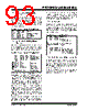
90 / 180 page  PIC16F627A/628A/648A DS40044D-page 88 © 2005 Microchip Technology Inc. 12.5.2 USART SYNCHRONOUS SLAVE RECEPTION The operation of the Synchronous Master and Slave modes is identical except in the case of the Sleep mode. Also, bit SREN is a “don’t care” in Slave mode. If receive is enabled by setting bit CREN prior to the SLEEP instruction, then a word may be received during Sleep. On completely receiving the word, the RSR register will transfer the data to the RCREG register and if enable bit RCIE bit is set, the interrupt generated will wake the chip from Sleep. If the global interrupt is enabled, the program will branch to the interrupt vector (0004h). Follow these steps when setting up a Synchronous Slave Reception: 1. TRISB<1> and TRISB<2> should both be set to ‘1’ to configure the RB1/RX/DT and RB2/TX/CK pins as inputs. Output drive, when required, is controlled by the peripheral circuitry. 2. Enable the synchronous master serial port by setting bits SYNC and SPEN and clearing bit CSRC. 3. If interrupts are desired, then set enable bit RCIE. 4. If 9-bit reception is desired, then set bit RX9. 5. To enable reception, set enable bit CREN. 6. Flag bit RCIF will be set when reception is complete and an interrupt will be generated, if enable bit RCIE was set. 7. Read the RCSTA register to get the ninth bit (if enabled) and determine if any error occurred during reception. 8. Read the 8-bit received data by reading the RCREG register. 9. If an OERR error occurred, clear the error by clearing bit CREN. TABLE 12-11: REGISTERS ASSOCIATED WITH SYNCHRONOUS SLAVE TRANSMISSION TABLE 12-12: REGISTERS ASSOCIATED WITH SYNCHRONOUS SLAVE RECEPTION Address Name Bit 7 Bit 6 Bit 5 Bit 4 Bit 3 Bit 2 Bit 1 Bit 0 Value on POR Value on all other Resets 0Ch PIR1 EEIF CMIF RCIF TXIF — CCP1IF TMR2IF TMR1IF 0000 -000 0000 -000 18h RCSTA SPEN RX9 SREN CREN ADEN FERR OERR RX9D 0000 000x 0000 000x 19h TXREG USART Transmit Data Register 0000 0000 0000 0000 8Ch PIE1 EEIE CMIE RCIE TXIE — CCP1IE TMR2IE TMR1IE 0000 -000 0000 -000 98h TXSTA CSRC TX9 TXEN SYNC — BRGH TRMT TX9D 0000 -010 0000 -010 99h SPBRG Baud Rate Generator Register 0000 0000 0000 0000 Legend: x = unknown, - = unimplemented read as ‘0’. Shaded cells are not used for synchronous slave transmission. Address Name Bit 7 Bit 6 Bit 5 Bit 4 Bit 3 Bit 2 Bit 1 Bit 0 Value on POR Value on all other Resets 0Ch PIR1 EEIF CMIF RCIF TXIF — CCP1IF TMR2IF TMR1IF 0000 -000 0000 -000 18h RCSTA SPEN RX9 SREN CREN ADEN FERR OERR RX9D 0000 000x 0000 000x 1Ah RCREG USART Receive Data Register 0000 0000 0000 0000 8Ch PIE1 EEIE CMIE RCIE TXIE — CCP1IE TMR2IE TMR1IE 0000 -000 0000 -000 98h TXSTA CSRC TX9 TXEN SYNC — BRGH TRMT TX9D 0000 -010 0000 -010 99h SPBRG Baud Rate Generator Register 0000 0000 0000 0000 Legend: x = unknown, - = unimplemented read as ‘0’. Shaded cells are not used for synchronous slave reception. |
|
ссылки URL |
| Вашему бизинису помогли Аллдатащит? [ DONATE ] |
Что такое Аллдатащит | реклама | контакт | Конфиденциальность | Ссылка на техническое описание | обмен ссыками | поиск по производителю All Rights Reserved©Alldatasheet.com |
| Russian : Alldatasheetru.com | Korean : Alldatasheet.co.kr | Spanish : Alldatasheet.es | French : Alldatasheet.fr | Italian : Alldatasheetit.com Portuguese : Alldatasheetpt.com | Polish : Alldatasheet.pl | Vietnamese : Alldatasheet.vn Indian : Alldatasheet.in | Mexican : Alldatasheet.com.mx | British : Alldatasheet.co.uk | New Zealand : Alldatasheet.co.nz |
|
Family Site : ic2ic.com |
icmetro.com |
 Russian ▼
 English
 Chinese
 German
 Japanese
 Russian
 Korean
 Spanish
 French
 Italian
 Portuguese
 Polish
 Vietnamese
 Indian
 Mexican
 British
 New Zealand