|
поискавой системы для электроныых деталей |
|
|
поискавой системы для электроныых деталей |
|
PIC16F627A датащи(PDF) 70 Page - Microchip Technology |
|
|
|||||||||||||||||||||||||||||
PIC16F627A датащи(HTML) 70 Page - Microchip Technology |
|
|
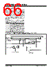
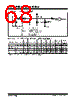
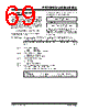
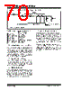
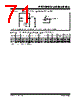
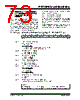
70 / 180 page  PIC16F627A/628A/648A DS40044D-page 68 © 2005 Microchip Technology Inc. FIGURE 11-1: VOLTAGE REFERENCE BLOCK DIAGRAM EXAMPLE 11-1: VOLTAGE REFERENCE CONFIGURATION 11.2 Voltage Reference Accuracy/Error The full range of VSS to VDD cannot be realized due to the construction of the module. The transistors on the top and bottom of the resistor ladder network (Figure 11-1) keep VREF from approaching VSS or VDD. The Voltage Reference module is VDD derived and therefore, the VREF output changes with fluctuations in VDD. The tested absolute accuracy of the Voltage Ref- erence module can be found in Table 17-3. 11.3 Operation During Sleep When the device wakes up from Sleep through an interrupt or a Watchdog Timer time out, the contents of the VRCON register are not affected. To minimize current consumption in Sleep mode, the Voltage Reference module should be disabled. 11.4 Effects of a Reset A device Reset disables the Voltage Reference module by clearing bit VREN (VRCON<7>). This Reset also disconnects the reference from the RA2 pin by clearing bit VROE (VRCON<6>) and selects the high voltage range by clearing bit VRR (VRCON<5>). The VREF value select bits, VRCON<3:0>, are also cleared. 11.5 Connection Considerations The Voltage Reference module operates independently of the Comparator module. The output of the reference generator may be connected to the RA2 pin if the TRISA<2> bit is set and the VROE bit, VRCON<6>, is set. Enabling the Voltage Reference module output onto the RA2 pin with an input signal present will increase current consumption. Connecting RA2 as a digital output with VREF enabled will also increase current consump- tion. The RA2 pin can be used as a simple D/A output with limited drive capability. Due to the limited drive capability, a buffer must be used in conjunction with the Voltage Reference module output for external connec- tions to VREF. Figure 11-2 shows an example buffering technique. Note: R is defined in Table 17-3. VRR 8R VR3 VR0 (From VRCON<3:0>) 16-1 Analog Mux 8R R R R R VREN VREF 16 Stages VDD VSS VSS MOVLW 0x02 ;4 Inputs Muxed MOVWF CMCON ;to 2 comps. BSF STATUS,RP0 ;go to Bank 1 MOVLW 0x07 ;RA3-RA0 are MOVWF TRISA ;outputs MOVLW 0xA6 ;enable VREF MOVWF VRCON ;low range set VR<3:0>=6 BCF STATUS,RP0 ;go to Bank 0 CALL DELAY10 ;10 μs delay |
|
ссылки URL |
| Вашему бизинису помогли Аллдатащит? [ DONATE ] |
Что такое Аллдатащит | реклама | контакт | Конфиденциальность | Ссылка на техническое описание | обмен ссыками | поиск по производителю All Rights Reserved©Alldatasheet.com |
| Russian : Alldatasheetru.com | Korean : Alldatasheet.co.kr | Spanish : Alldatasheet.es | French : Alldatasheet.fr | Italian : Alldatasheetit.com Portuguese : Alldatasheetpt.com | Polish : Alldatasheet.pl | Vietnamese : Alldatasheet.vn Indian : Alldatasheet.in | Mexican : Alldatasheet.com.mx | British : Alldatasheet.co.uk | New Zealand : Alldatasheet.co.nz |
|
Family Site : ic2ic.com |
icmetro.com |
 Russian ▼
 English
 Chinese
 German
 Japanese
 Russian
 Korean
 Spanish
 French
 Italian
 Portuguese
 Polish
 Vietnamese
 Indian
 Mexican
 British
 New Zealand