|
поискавой системы для электроныых деталей |
|
|
поискавой системы для электроныых деталей |
|
PIC16F627A датащи(PDF) 64 Page - Microchip Technology |
|
|
|||||||||||||||||||||||||||||
PIC16F627A датащи(HTML) 64 Page - Microchip Technology |
|
|
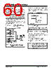
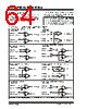
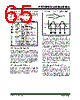
64 / 180 page  PIC16F627A/628A/648A DS40044D-page 62 © 2005 Microchip Technology Inc. 10.1 Comparator Configuration There are eight modes of operation for the comparators. The CMCON register is used to select the mode. Figure 10-1 shows the eight possible modes. The TRISA register controls the data direction of the comparator pins for each mode. If the Comparator mode is changed, the comparator output level may not be valid for the specified mode change delay shown in Table 17-2. FIGURE 10-1: COMPARATOR I/O OPERATING MODES Note 1: Comparator interrupts should be disabled during a Comparator mode change, otherwise a false interrupt may occur. 2: Comparators can have an inverted output. See Figure 10-1. C1 RA0/AN0 VIN- VIN+ RA3/AN3/CMP1 Comparators Reset (POR Default Value) A A CM<2:0> = 000 C2 RA1/AN1 VIN- VIN+ RA2/AN2/VREF A A C1 RA0/AN0 VIN- VIN+ RA3/AN3/CMP1 Two Independent Comparators A A CM<2:0> = 100 C2 RA1/AN1 VIN- VIN+ RA2/AN2/VREF A A C1 RA0/AN0 VIN- VIN+ RA3/AN3/CMP1 Two Common Reference Comparators A D CM<2:0> = 011 C2 RA1/AN1 VIN- VIN+ RA2/AN2/VREF A A C1 RA0/AN0 VIN- VIN+ RA3/AN3/CMP1 Off (Read as ‘0’) One Independent Comparator D D CM<2:0> = 101 C2 RA1/AN1 VIN- VIN+ RA2/AN2/VREF A A C1 VIN- VIN+ Off (Read as ‘0’) Comparators Off D D CM<2:0> = 111 C2 VIN- VIN+ Off (Read as ‘0’) D D C1 RA0/AN0 VIN- VIN+ RA3/AN3/CMP1 Four Inputs Multiplexed to Two Comparators A A CM<2:0> = 010 C2 RA1/AN1 VIN- VIN+ RA2/AN2/VREF A A From VREF CIS = 0 CIS = 1 CIS = 0 CIS = 1 C1 RA0/AN0 VIN- VIN+ RA3/AN3/CMP1 Two Common Reference Comparators with Outputs A D CM<2:0> = 110 C2 RA1/AN1 VIN- VIN+ RA2/AN2/VREF A A Open Drain A = Analog Input, port reads zeros always. D = Digital Input. CIS (CMCON<3>) is the Comparator Input Switch. RA4/T0CKI/CMP2 C1 RA0/AN0 VIN- VIN+ RA3/AN3/CMP1 Three Inputs Multiplexed to Two Comparators A A CM<2:0> = 001 C2 RA1/AN1 VIN- VIN+ RA2/AN2/VREF A A CIS = 0 CIS = 1 VSS VSS RA0/AN0 RA3/AN3/CMP1 RA1/AN1 RA2/AN2/VREF Module C1VOUT C2VOUT C1VOUT C2VOUT Off (Read as ‘0’) Off (Read as ‘0’) C2VOUT C1VOUT C2VOUT C1VOUT C2VOUT C1VOUT C2VOUT |
|
ссылки URL |
| Вашему бизинису помогли Аллдатащит? [ DONATE ] |
Что такое Аллдатащит | реклама | контакт | Конфиденциальность | Ссылка на техническое описание | обмен ссыками | поиск по производителю All Rights Reserved©Alldatasheet.com |
| Russian : Alldatasheetru.com | Korean : Alldatasheet.co.kr | Spanish : Alldatasheet.es | French : Alldatasheet.fr | Italian : Alldatasheetit.com Portuguese : Alldatasheetpt.com | Polish : Alldatasheet.pl | Vietnamese : Alldatasheet.vn Indian : Alldatasheet.in | Mexican : Alldatasheet.com.mx | British : Alldatasheet.co.uk | New Zealand : Alldatasheet.co.nz |
|
Family Site : ic2ic.com |
icmetro.com |
 Russian ▼
 English
 Chinese
 German
 Japanese
 Russian
 Korean
 Spanish
 French
 Italian
 Portuguese
 Polish
 Vietnamese
 Indian
 Mexican
 British
 New Zealand