|
поискавой системы для электроныых деталей |
|
|
поискавой системы для электроныых деталей |
|
ADP1050ACPZ-R7 датащи(PDF) 16 Page - Analog Devices |
|
|
|||||||||||||||||||||||||||||
ADP1050ACPZ-R7 датащи(HTML) 16 Page - Analog Devices |
|
|
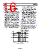
16 / 93 page  Data Sheet ADP1050 The ADP1050 synchronizes to the external clock frequency as follows: 1. After the synchronization function is enabled by Register 0xFE12[3] and Register 0xFE12[0], the ADP1050 starts to detect the period of the external clock signal applied at the SYNI/FLGI pin. 2. If all periods of the most recent 64 consecutive cycles of the external clocks fall within 90% to 110% of the internal switching clock period, the ADP1050 uses the latest current cycle as the synchronization reference, and the period of the external clock is identified. This interval is t2 or t4, as shown in Figure 15. Otherwise, the ADP1050 discards this cycle and looks for the next cycle (frequency capture mode). 3. After the external clock period is determined, the ADP1050 detects the phase shift between the external clock (plus the delay time set by Register 0xFE11) and the internal PWM signal. If the phase shift is within the phase capture range, the internal and external clocks are synchronized (phase capture mode). 4. The PWM clock is synchronized with the external clock. Cycle- by-cycle synchronization starts. 5. If the external clock signal is lost at any time, or if the period exceeds the minimum limit (89% of the internal programmed frequency) or the maximum limit (114% of the internal programmed frequency), the ADP1050 takes the last valid external clock signal as the synchronization reference source. At the same time, the phase shift between the synchronization reference and the internal clock is detected. When the phase shift falls within the phase capture range, the PWM clock returns to the internal clock set by the internal oscillator. This interval is t1 or t3, as shown in Figure 15. This is the first synchronization unlock condition, called Synchronization Unlocked Mode 1, in which the switching frequency is out of range (range is 89% to approximately 114% of the internal programmed frequency). 6. If the period of the external SYNI signal changes significantly (for example, if the period difference between contiguous cycles exceeds 280 ns), the ADP1050 takes the last valid external clock signal as the synchronization reference source. At the same time, the phase shift between the synchronization reference and the internal clock is detected. When the phase shift falls within the phase capture range, the PWM clock returns to the internal clock set by the internal oscillator. This is the second synchronization unlock condition, called Synchronization Unlocked Mode 2, in which the phase shift exceeds 280 ns. Figure 15 shows the synchronization operation diagram. The internal frequency, fSW_INT, is the internal free-running frequency of the ADP1050. Before the synchronization is locked, the ADP1050 runs at fSW_INT. The external frequency, fSW_EXT, is the frequency of the external clock to which the ADP1050 must synchronize. After synchronization is locked, the ADP1050 runs at fSW_EXT. The ADP1050 does not allow the switching frequency to cross the boundaries of 97.5 kHz, 195.5 kHz, or 390.5 kHz on-the-fly. Ensure that the external clock does not cross these boundaries. Otherwise, the internal switching frequency cannot be set within ±10% of these boundaries. UNIT OFF UNIT ON UNIT ON TIME EXTERNAL CLOCK FREQUENCY (fSW_EXT) OPERATING SWITCHING FREQUENCY INTERNAL CLOCK FREQUENCY (fSW_INT) t1 t2 t4 t3 fSW 110% fSW_INT 114% fSW_INT fSW_INT 90% fSW_INT 89% fSW_INT Figure 15. Synchronization Operation Rev. A | Page 15 of 92 |
|
ссылки URL |
| Вашему бизинису помогли Аллдатащит? [ DONATE ] |
Что такое Аллдатащит | реклама | контакт | Конфиденциальность | Ссылка на техническое описание | обмен ссыками | поиск по производителю All Rights Reserved©Alldatasheet.com |
| Russian : Alldatasheetru.com | Korean : Alldatasheet.co.kr | Spanish : Alldatasheet.es | French : Alldatasheet.fr | Italian : Alldatasheetit.com Portuguese : Alldatasheetpt.com | Polish : Alldatasheet.pl | Vietnamese : Alldatasheet.vn Indian : Alldatasheet.in | Mexican : Alldatasheet.com.mx | British : Alldatasheet.co.uk | New Zealand : Alldatasheet.co.nz |
|
Family Site : ic2ic.com |
icmetro.com |
 Russian ▼
 English
 Chinese
 German
 Japanese
 Russian
 Korean
 Spanish
 French
 Italian
 Portuguese
 Polish
 Vietnamese
 Indian
 Mexican
 British
 New Zealand