|
поискавой системы для электроныых деталей |
|
|
поискавой системы для электроныых деталей |
|
ADP1050ACPZ-R7 датащи(PDF) 88 Page - Analog Devices |
|
|
|||||||||||||||||||||||||||||
ADP1050ACPZ-R7 датащи(HTML) 88 Page - Analog Devices |
|
|
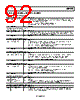
88 / 93 page  Data Sheet ADP1050 Table 154. Register 0xFE65—Current Value Update Rate Setting Bits Bit Name/Function R/W Description [7:2] Reserved R/W Reserved. [1:0] Current value update rate R/W These bits specify the update rate for the current value of CS1 (READ_IIN command, Register 0x89). By default, the current values are updated every 10 ms. Bit 1 Bit 0 CS1 Value Update Rate (ms) 0 0 10 (defaut) 0 1 52 1 0 105 1 1 210 Table 155. Register 0xFE67—Open-Loop Operation Settings Bits Bit Name/Function R/W Description 7 Reserved R Reserved. 6 Pulse skipping mode enable R/W 1 = enables pulse skipping mode. If the ADP1050 requires a modulation value that is less than the threshold set by Register 0xFE69, pulse skipping is in use. 5 SR2 open-loop operation enable R/W This bit is set when SR2 is used in open-loop operation mode. 4 SR1 open-loop operation enable R/W This bit is set when SR1 is used in open-loop operation mode. 3 Reserved R/W Reserved. 2 Reserved R/W Reserved. 1 OUTB open-loop operation enable R/W This bit is set when OUTB is used in open-loop operation mode. 0 OUTA open-loop operation enable R/W This bit is set when OUTA is used in open-loop operation mode. Table 156. Register 0xFE69—Pulse Skipping Mode Threshold Bits Bit Name/Function R/W Description [7:0] Pulse skipping mode threshold R/W These bits set the modulation pulse width threshold for pulse skipping. Each LSB is 5 ns. Table 157. Register 0xFE6A—CS3_OC_FAULT_LIMIT Bits Bit Name/Function R/W Description [7:0] CS3_OC_FAULT_LIMIT R/W The eight MSB value of the CS3 value register in Register 0xFEA9 is compared with this 8-bit number. If the 8 MSB value is greater, the CS3_OC_FAULT flag is set. Table 158. Register 0xFE6B—Modulation Threshold for OVP Selection Bits Bit Name/Function R/W Description [7:0] Modulation threshold for conditional OVP responses R/W This value sets modulation threshold for conditional OVP response. When the real-time modulation value is above this threshold, the LARGE_MODULATION flag in Register 0xFE6C[2] is set. Switching Frequency Range (kHz) Resolution Corresponding to LSB (ns) 49 to 87 80 97.5 to 184 40 195.5 to 379 20 390.5 to 625 10 Rev. A | Page 87 of 92 |
|
ссылки URL |
| Вашему бизинису помогли Аллдатащит? [ DONATE ] |
Что такое Аллдатащит | реклама | контакт | Конфиденциальность | Ссылка на техническое описание | обмен ссыками | поиск по производителю All Rights Reserved©Alldatasheet.com |
| Russian : Alldatasheetru.com | Korean : Alldatasheet.co.kr | Spanish : Alldatasheet.es | French : Alldatasheet.fr | Italian : Alldatasheetit.com Portuguese : Alldatasheetpt.com | Polish : Alldatasheet.pl | Vietnamese : Alldatasheet.vn Indian : Alldatasheet.in | Mexican : Alldatasheet.com.mx | British : Alldatasheet.co.uk | New Zealand : Alldatasheet.co.nz |
|
Family Site : ic2ic.com |
icmetro.com |
 Russian ▼
 English
 Chinese
 German
 Japanese
 Russian
 Korean
 Spanish
 French
 Italian
 Portuguese
 Polish
 Vietnamese
 Indian
 Mexican
 British
 New Zealand