|
поискавой системы для электроныых деталей |
|
|
поискавой системы для электроныых деталей |
|
ADP1050ACPZ-R7 датащи(PDF) 81 Page - Analog Devices |
|
|
|||||||||||||||||||||||||||||
ADP1050ACPZ-R7 датащи(HTML) 81 Page - Analog Devices |
|
|
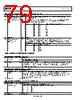
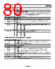
81 / 93 page  ADP1050 Data Sheet Table 127. Register 0xFE2D—RTD Current Source Settings Bits Bit Name/Function R/W Description [7:6] RTD current setting R/W These bits set the size of the current source on the RTD pin. Bit 7 Bit 6 Current Source (µA) 0 0 10 0 1 20 1 0 30 1 1 40 [5:0] RTD current trim R/W These six bits are used to trim the current source on the RTD pin. Each LSB corresponds to 160 nA, independent of the RTD current setting selected in Bits[7:6]. Table 128. Register 0xFE2F—OT Hysteresis Settings Bits Bit Name/Function R/W Description [7:3] Reserved R/W Reserved. 2 OT_WARNING flag debounce R/W This bit sets the OT_WARNING flag debounce time. 0 = sets the flag actions debounce time to 100 ms. 1 = sets the flag actions debounce time to 0 ms. [1:0] OT hysteresis R/W These bits set the OT hysteresis. Due to the negative temperature coefficient of the NTC thermistor or analog temperature sensor, the OT_FAULT flag clearing voltage threshold is programmed with a voltage greater than the OT_FAULT flag setting voltage threshold. Bit 1 Bit 0 OT Hysteresis 0 0 OT hysteresis = 12.5 mV (4 LSBs) 0 1 OT hysteresis = 25 mV (8 LSBs) 1 0 OT hysteresis = 37.5 mV (12 LSBs) 1 1 OT hysteresis = 50 mV (16 LSBs) DIGITAL COMPENSATOR AND MODULATION SETTING REGISTERS POLE LOCATION RANGE ZERO 100Hz 500Hz 1kHz 5kHz 10kHz POLE LF FILTER HF FILTER Figure 56. Digital Compensator Programmability Table 129. Register 0xFE30—Normal Mode Compensator Low Frequency Gain Settings Bits Bit Name/Function R/W Description [7:0] Normal mode low frequency gain R/W This register determines the low frequency gain of the digital compensator in normal mode. It is programmable over a 48.13 dB range. See Figure 56. Table 130. Register 0xFE31—Normal Mode Compensator Zero Settings Bits Bit Name/Function R/W Description [7:0] Normal mode zero settings R/W This register determines the position of the zero of the digital compensator in normal mode. See Figure 56. Rev. A | Page 80 of 92 |
|
ссылки URL |
| Вашему бизинису помогли Аллдатащит? [ DONATE ] |
Что такое Аллдатащит | реклама | контакт | Конфиденциальность | Ссылка на техническое описание | обмен ссыками | поиск по производителю All Rights Reserved©Alldatasheet.com |
| Russian : Alldatasheetru.com | Korean : Alldatasheet.co.kr | Spanish : Alldatasheet.es | French : Alldatasheet.fr | Italian : Alldatasheetit.com Portuguese : Alldatasheetpt.com | Polish : Alldatasheet.pl | Vietnamese : Alldatasheet.vn Indian : Alldatasheet.in | Mexican : Alldatasheet.com.mx | British : Alldatasheet.co.uk | New Zealand : Alldatasheet.co.nz |
|
Family Site : ic2ic.com |
icmetro.com |
 Russian ▼
 English
 Chinese
 German
 Japanese
 Russian
 Korean
 Spanish
 French
 Italian
 Portuguese
 Polish
 Vietnamese
 Indian
 Mexican
 British
 New Zealand