|
поискавой системы для электроныых деталей |
|
|
поискавой системы для электроныых деталей |
|
ADP1050ACPZ-R7 датащи(PDF) 72 Page - Analog Devices |
|
|
|||||||||||||||||||||||||||||
ADP1050ACPZ-R7 датащи(HTML) 72 Page - Analog Devices |
|
|
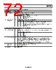
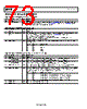
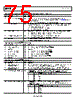
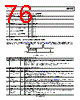
72 / 93 page  Data Sheet ADP1050 Table 98. Register 0xFE03—Flag Response, FLAGIN_RESPONSE Bits Bit Name/Function R/W Description [7:4] Reserved R/W Reserved. [3:2] Fault response R/W These bits specify the action when the flag is set. Bit 3 Bit 2 Fault Response 0 0 Continues operation without interruption. 0 1 Disable SR1 and SR2. 1 0 Disable all PWM outputs. 1 1 Reserved. [1:0] Action after the fault flag is cleared R/W These bits specify the action when the flag is cleared. Bit 1 Bit 0 Action After Fault Flag Clears 0 0 After the flag reenable delay time, the PWM outputs are reenabled with a soft start. 0 1 The PWM outputs are reenabled immediately without a soft start. 1 0 A PSON signal, programmed in Register 0x01, Register 0x02, and/or the CTRL pin, is needed to reenable the PWM outputs. 1 1 Reserved. Table 99. Register 0xFE05—Flag Reenable Delay, VDD_OV_RESPONSE Bits Bit Name/Function R/W Description [7:6] Flag reenable delay R/W These bits specify the global delay from the time when a manufacturer specific flag is cleared to the soft start. Bit 7 Bit 6 Typical Delay Time 0 0 250 ms 0 1 500 ms 1 0 1 sec 1 1 2 sec 5 VDD_OV flag ignore R/W This bit enables or disables the VDD_OV flag. 0 = VDD_OV flag is set when there is a VDD overvoltage condition. When there is a VDD overvoltage condition, the flag is set and the ADP1050 shuts down. When the VDD overvoltage condition ends, the flag is cleared and the device downloads the EEPROM contents before restarting with a soft start process. 1 = VDD_OV flag is always cleared. When there is a VDD overvoltage condition, the flag is always cleared and the device continues to operate without interruption. 4 VDD_OV flag debounce R/W This bit sets the debounce time for the VDD_OV flag. 0 = 500 μs debounce time. 1 = 2 μs debounce time. [3:0] Reserved R/W Reserved. Rev. A | Page 71 of 92 |
|
ссылки URL |
| Вашему бизинису помогли Аллдатащит? [ DONATE ] |
Что такое Аллдатащит | реклама | контакт | Конфиденциальность | Ссылка на техническое описание | обмен ссыками | поиск по производителю All Rights Reserved©Alldatasheet.com |
| Russian : Alldatasheetru.com | Korean : Alldatasheet.co.kr | Spanish : Alldatasheet.es | French : Alldatasheet.fr | Italian : Alldatasheetit.com Portuguese : Alldatasheetpt.com | Polish : Alldatasheet.pl | Vietnamese : Alldatasheet.vn Indian : Alldatasheet.in | Mexican : Alldatasheet.com.mx | British : Alldatasheet.co.uk | New Zealand : Alldatasheet.co.nz |
|
Family Site : ic2ic.com |
icmetro.com |
 Russian ▼
 English
 Chinese
 German
 Japanese
 Russian
 Korean
 Spanish
 French
 Italian
 Portuguese
 Polish
 Vietnamese
 Indian
 Mexican
 British
 New Zealand