|
поискавой системы для электроныых деталей |
|
|
поискавой системы для электроныых деталей |
|
L9908 датащи(PDF) 67 Page - STMicroelectronics |
|
|
|||||||||||||||||||||||||||||
L9908 датащи(HTML) 67 Page - STMicroelectronics |
|
|
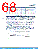
67 / 153 page  Figure 39. VGS Monitor operative ranges 5.12.2 Dead Time Protection (DTP) The prevention of cross-conduction due to HSn/LSn ON-phase overlap is in principle under the responsibility of the uC driving the PWM pins INHn/INLn. However, a built-in dead time protection is available. When the main logic processes a falling edge event on INHn/INLn it starts a programmable masking time interval T_dead_flt during which the rising edges on the opposite signal (INLn/INHn respectively) are ignored. In general a rising edge on INHn/INLn is processed only during the condition INHn=INLn= 0 and if such a condition hold for at least a T_dead_flt. Figure 40. Dead Time Protection functional operation The T_dead_flt configuration can be set by the dedicated SPI signal DTP_CFG within the register GEN_CFG1 as follows: Table 61. Dead Time Protection configuration bits DTP_CFG2 DTP_CFG1 DTP_CFG0 Description 0 0 0 0us – DTP Disabled 0 0 1 0.25 μs L9908 Half bridges gate drivers DS13546 - Rev 3 page 67/153 |
|
ссылки URL |
| Вашему бизинису помогли Аллдатащит? [ DONATE ] |
Что такое Аллдатащит | реклама | контакт | Конфиденциальность | Ссылка на техническое описание | обмен ссыками | поиск по производителю All Rights Reserved©Alldatasheet.com |
| Russian : Alldatasheetru.com | Korean : Alldatasheet.co.kr | Spanish : Alldatasheet.es | French : Alldatasheet.fr | Italian : Alldatasheetit.com Portuguese : Alldatasheetpt.com | Polish : Alldatasheet.pl | Vietnamese : Alldatasheet.vn Indian : Alldatasheet.in | Mexican : Alldatasheet.com.mx | British : Alldatasheet.co.uk | New Zealand : Alldatasheet.co.nz |
|
Family Site : ic2ic.com |
icmetro.com |
 Russian ▼
 English
 Chinese
 German
 Japanese
 Russian
 Korean
 Spanish
 French
 Italian
 Portuguese
 Polish
 Vietnamese
 Indian
 Mexican
 British
 New Zealand