|
поискавой системы для электроныых деталей |
|
|
поискавой системы для электроныых деталей |
|
L9908 датащи(PDF) 65 Page - STMicroelectronics |
|
|
|||||||||||||||||||||||||||||
L9908 датащи(HTML) 65 Page - STMicroelectronics |
|
|
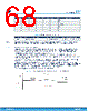
65 / 153 page  Figure 37. Ext. FET Turn-on/off simplified behavior Where: 1. The gate-source voltage (VGS) ramps up according to the time constant formed by the FET gate resistance (Rg) and input capacitance (Ciss) 2. Once the VGS reaches the threshold voltage (Vth) the current through the device starts to ramp up. The channel is supporting the full-load current and the drain-source voltage (VDS) starts decaying. 3. The VDS falls continuously to its on-state value while the VGS stays approximately constant (Miller Plateau) as well as the gate current. 4. The VGS ramps up to the value applied by the driver. This additional gate voltage fully enhances the FET channel and reaches the full RdsON. Turn-off is the reverse of turn-on process. During turn-off, the Miller Plateau indicates the start of the rise of the VDS and the voltage of the Miller Plateau will represent the minimum required VGS to sustain the load current. While a precise value of FET`s VDS slew rates at turn-on/off requires simulations including FET and GDU model plus the board and package parasitic details a first order approximations can be used to estimate this value. The key parameter required for the estimation is the peak current the driver can source/sink to the Ext. FET gate terminal during the turn-on/off process, so the FET VDS rise/fall time can then be approximated by: trise= Qgd IDRV_SOURCE_PEAK (6) tfall= Qgd IDRV_SINK_PEAK (7) Where Qgd is the Ext. FET gate-drain charge and Idrv_source/sink_peak are the predrivers Pull-up/Pull-down current. Driver peak current should not be confused with drivers Average Current which is the average current the driver is delivering over full FET switching period i.e. IDRV_AVERAGE=Qgfsw (8) Where Qg is the Ext. FET total gate charge and fsw is the predriver switching frequency. Output peak current limitation Since pre-drivers output current is not programmable the peak level can be reduced by means of an external series resistances in order to achieve the following goals: • dump ringing due to parasitic inductances/capacitances; • dump ringing due to high voltage/current switching dv/dt, di/dt, and Ext. FET’s body-diode reverse recovery charge; • optimize the switching losses; • reduce electromagnetic interference (EMI). L9908 Half bridges gate drivers DS13546 - Rev 3 page 65/153 |
|
ссылки URL |
| Вашему бизинису помогли Аллдатащит? [ DONATE ] |
Что такое Аллдатащит | реклама | контакт | Конфиденциальность | Ссылка на техническое описание | обмен ссыками | поиск по производителю All Rights Reserved©Alldatasheet.com |
| Russian : Alldatasheetru.com | Korean : Alldatasheet.co.kr | Spanish : Alldatasheet.es | French : Alldatasheet.fr | Italian : Alldatasheetit.com Portuguese : Alldatasheetpt.com | Polish : Alldatasheet.pl | Vietnamese : Alldatasheet.vn Indian : Alldatasheet.in | Mexican : Alldatasheet.com.mx | British : Alldatasheet.co.uk | New Zealand : Alldatasheet.co.nz |
|
Family Site : ic2ic.com |
icmetro.com |
 Russian ▼
 English
 Chinese
 German
 Japanese
 Russian
 Korean
 Spanish
 French
 Italian
 Portuguese
 Polish
 Vietnamese
 Indian
 Mexican
 British
 New Zealand