|
поискавой системы для электроныых деталей |
|
|
поискавой системы для электроныых деталей |
|
ADF4252BCPZ-R7 датащи(PDF) 24 Page - Analog Devices |
|
|
|||||||||||||||||||||||||||||
ADF4252BCPZ-R7 датащи(HTML) 24 Page - Analog Devices |
|
|
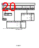
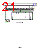
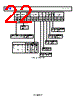
24 / 30 page  ADF4252 Data Sheet Rev. E | Page 24 of 30 RF Charge Pump Three-State This bit puts the charge pump into three-state mode when programmed to a 1. It must be set to 0 for normal operation. RF Power-Down DB5 on the ADF4252 provides the programmable power-down mode. Setting this bit to a 1 performs a power-down on both the RF and IF sections. Setting this bit to 0 returns the RF and IF sections to normal operation. While in software power- down, the device retains all information in its registers. Only when supplies are removed are the register contents lost. When a power-down is activated, the following events occur: 1. All active RF dc current paths are removed. 2. The RF synthesizer counters are forced to their load state conditions. 3. The RF charge pump is forced into three-state mode. 4. The RF digital lock detect circuitry is reset. 5. The RFIN input is debiased. 6. The input register remains active and capable of loading and latching data. RF Phase Detector Polarity DB7 on the ADF4252 sets the RF phase detector polarity. When the VCO characteristics are positive, this bit must be set to 1. When VCO characteristics are negative, this bit must be set to 0. RF Charge Pump Current Setting DB9 and DB10 set the RF charge pump current setting. This must be set to whatever charge pump current the loop filter has been designed with (see Figure 37). RF Test Modes These bits must be set to 000 for normal operation. MASTER REGISTER (ADDRESS R3) With Bits[2:0] of R3 set to 011, the on-chip master register is programmed. Figure 38 shows the input data format for programming the master register. RF and IF Counter Reset DB3 is the counter reset bit for the ADF4252. When this bit is 1, both the RF and IF R, INT, and MOD counters are held in reset. For normal operation, this bit must be 0. Upon power-up, the DB3 bit must be disabled, and the INT counter resumes counting in close alignment with the R counter (the maximum error is one prescaler cycle). Charge Pump Three-State This bit puts both the RF and IF charge pump into three-state mode when programmed to a 1. It must be set to 0 for normal operation. Power-Down Bit 3 of R3 on the ADF4252 provides the programmable power- down mode. Setting this bit to a 1 performs a power-down on both the RF and IF sections. Setting this bit to 0 returns the RF and IF sections to normal operation. While in software power- down, the device retains all information in its registers. Only when supplies are removed are the register contents lost. When a power-down is activated, the following events occur: 1. All active dc current paths are removed. 2. The RF and IF counters are forced to their load state conditions. 3. The RF and IF charge pumps are forced into three-state mode. 4. The digital lock detect circuitry is reset. 5. The RFIN input and IFIN input are debiased. 6. The oscillator input buffer circuitry is disabled. 7. The input register remains active and capable of loading and latching data. XO Disable Setting this bit to 1 disables the REFOUT circuitry. This is set to 1 when using an external TCXO, VCXO, or other reference sources. This is set to 0 when using the REFIN and REFOUT pins to form an oscillator circuit. MUXOUT Control The on-chip multiplexer is controlled by Bits[10: 7] of R3 on the ADF4252. Figure 38 shows the truth table. If the user updates the RF control register or the IF control register, the MUXOUT contents are lost. To retrieve the MUXOUT signal, the user must write to the master register. Lock Detect The digital lock detect output goes high if there are 40 successive PFD cycles with an input error of less than 15 ns. It stays high until a new channel is programmed or until the error at the PFD input exceeds 30 ns for one or more cycles. If the loop bandwidth is narrow compared to the PFD frequency, the error at the PFD inputs may drop below 15 ns for 40 cycles around a cycle slip; therefore, the digital lock detect may go falsely high for a short period until the error again exceeds 30 ns. In this case, the digital lock detect is reliable only as a loss of lock indicator. IF N DIVIDER REGISTER (ADDRESS R4) With Bits[2:0] of R4 set to 100, the on-chip IF N divider register is programmed. Figure 39 shows the input data format for programming this register. IF CP Gain When set to 1, this bit changes the IF charge pump current setting to its maximum value. When the bit is set to 0, the charge pump current reverts back to its previous state. IF Prescaler The dual-modulus prescaler (P/P + 1), along with the IF A and IF B counters, determine the overall division ratio, N, to be realized (N = PB + A) from the IFIN to the IF PFD input. Operating at CML levels, the prescaler takes the clock from the IF input stage and divides it down to a manageable frequency for the CMOS counters. It is based on a synchronous 4/5 core. See Equation 2 and Figure 39. |
|
ссылки URL |
| Вашему бизинису помогли Аллдатащит? [ DONATE ] |
Что такое Аллдатащит | реклама | контакт | Конфиденциальность | Ссылка на техническое описание | обмен ссыками | поиск по производителю All Rights Reserved©Alldatasheet.com |
| Russian : Alldatasheetru.com | Korean : Alldatasheet.co.kr | Spanish : Alldatasheet.es | French : Alldatasheet.fr | Italian : Alldatasheetit.com Portuguese : Alldatasheetpt.com | Polish : Alldatasheet.pl | Vietnamese : Alldatasheet.vn Indian : Alldatasheet.in | Mexican : Alldatasheet.com.mx | British : Alldatasheet.co.uk | New Zealand : Alldatasheet.co.nz |
|
Family Site : ic2ic.com |
icmetro.com |
 Russian ▼
 English
 Chinese
 German
 Japanese
 Russian
 Korean
 Spanish
 French
 Italian
 Portuguese
 Polish
 Vietnamese
 Indian
 Mexican
 British
 New Zealand