|
поискавой системы для электроныых деталей |
|
|
поискавой системы для электроныых деталей |
|
ADF4252BCPZ-R7 датащи(PDF) 23 Page - Analog Devices |
|
|
|||||||||||||||||||||||||||||
ADF4252BCPZ-R7 датащи(HTML) 23 Page - Analog Devices |
|
|
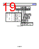
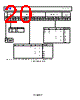
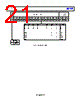
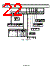
23 / 30 page  Data Sheet ADF4252 Rev. E | Page 23 of 30 REGISTER DESCRIPTIONS RF N DIVIDER REGISTER (ADDRESS R0) With Bits[2:0] of R0 set to 000, the on-chip RF N divider register is programmed. Figure 35 shows the input data format for programming this register. 8-Bit RF INT Value These eight bits control what is loaded as the INT value. INT is used to determine the overall feedback division factor. It is used in Equation 1. 12-Bit RF FRAC Value These 12 bits control what is loaded as the FRAC value into the fractional interpolator. FRAC is part of what determines the overall feedback division factor. It is used in Equation 1. The FRAC value must be less than or equal to the value loaded into the MOD register. RF R DIVIDER REGISTER (ADDRESS R1) With Bits[2:0] of R1 set to 001, the on-chip RF R divider register is programmed. Figure 36 shows the input data format for programming this register. RF Prescaler (P/P + 1) The RF dual-modulus prescaler (P/P +1), along with the INT, FRAC, and MOD counters, determine the overall division ratio from the RFIN to the PFD input. Operating at CML levels, the prescaler takes the clock from the RF input stage and divides it down to a manageable frequency for the CMOS counters. The prescaler is based on a synchronous 4/5 core (see Figure 36). RF REFIN Doubler Setting this bit to 0 feeds the REFIN signal directly to the 4-bit RF R counter, disabling the doubler. Setting this bit to 1 multiplies the REFIN frequency by a factor of 2 before feeding into the 4-bit RF R counter. When the doubler is disabled, the REFIN falling edge is the active edge at the PFD input to the fractional-N synthesizer. When the doubler is enabled, both the rising and falling edges of REFIN become active edges at the PFD input. When the doubler is enabled and lowest spur mode is chosen, the in-band phase noise performance is sensitive to the REFIN duty cycle. The phase noise degradation can be as much as 5 dB for REFIN duty cycles outside a 45% to 55% range. The phase noise is insensitive to REFIN duty cycle in the lowest noise mode and in low noise and spur mode. The phase noise is insensitive to the REFIN duty cycle when the doubler is disabled. 4-Bit RF R Counter The 4-bit RF R counter allows the input reference frequency (REFIN) to be divided down to produce the reference clock to the phase frequency detector (PFD). Division ratios from 1 to 15 are allowed. 12-Bit Interpolator Modulus This programmable register sets the fractional modulus. The fractional modulus is the ratio of the PFD frequency to the channel step resolution on the RF output. RF CONTROL REGISTER (ADDRESS R2) With Bits[2:0] of R2 set to 010, the on-chip RF control register is programmed. Figure 37 shows the input data format for programming this register. Upon initialization, DB15 to DB11 must all be set to 0. Noise and Spur Setting The noise and spur setting (Bit 15, Bit 11, and Bit 06 of R2) is a feature that allows the user to optimize his or her design either for improved spurious performance or for improved phase noise performance. When set to 000, the lowest spurs setting is chosen. In this setting, dither is enabled. This randomizes the fractional quantization noise so that it looks more like white noise than spurious noise, which means that the device is optimized for improved spurious performance. This operation is normally used when the PLL closed-loop bandwidth is wide for fast locking applications. A wide-loop filter does not attenuate the spurs to a level that a narrow-loop bandwidth does. When these bits are set to 001, the low noise and spur setting is enabled. In this setting, dither is disabled. This optimizes the synthesizer to operate with improved noise performance. However, the spurious performance is degraded in this mode compared to the lowest spurs setting. To improve noise performance even further, another option is available that reduces the phase noise. This is the lowest noise setting: 111. As well as disabling the dither, it also ensures that the charge pump is operating in an optimum region for noise performance. This setting is extremely useful where a narrow-loop filter bandwidth is available. The synthesizer ensures extremely low noise, and the filter attenuates the spurs. The Typical Performance Characteristics section gives the user an idea of the trade-off in a typical WCDMA setup for the different noise and spur settings. RF Counter Reset DB3 is the RF counter reset bit for the ADF4252. When this bit is 1, the RF synthesizer counters are held in reset. For normal operation, this bit must be 0. |
|
ссылки URL |
| Вашему бизинису помогли Аллдатащит? [ DONATE ] |
Что такое Аллдатащит | реклама | контакт | Конфиденциальность | Ссылка на техническое описание | обмен ссыками | поиск по производителю All Rights Reserved©Alldatasheet.com |
| Russian : Alldatasheetru.com | Korean : Alldatasheet.co.kr | Spanish : Alldatasheet.es | French : Alldatasheet.fr | Italian : Alldatasheetit.com Portuguese : Alldatasheetpt.com | Polish : Alldatasheet.pl | Vietnamese : Alldatasheet.vn Indian : Alldatasheet.in | Mexican : Alldatasheet.com.mx | British : Alldatasheet.co.uk | New Zealand : Alldatasheet.co.nz |
|
Family Site : ic2ic.com |
icmetro.com |
 Russian ▼
 English
 Chinese
 German
 Japanese
 Russian
 Korean
 Spanish
 French
 Italian
 Portuguese
 Polish
 Vietnamese
 Indian
 Mexican
 British
 New Zealand