|
поискавой системы для электроныых деталей |
|
|
поискавой системы для электроныых деталей |
|
ADP5600ACPZ-R7 датащи(PDF) 23 Page - Analog Devices |
|
|
|||||||||||||||||||||||||||||
ADP5600ACPZ-R7 датащи(HTML) 23 Page - Analog Devices |
|
|
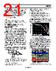
23 / 25 page  Data Sheet ADP5600 Rev. 0 | Page 23 of 25 DESIGN EXAMPLE This section provides an example of the step by step design procedures and the external components required for ADP5600. Table 9 lists the design requirements for this example. Table 9. Example Design Requirements for ADP5600 Parameter Specification LDO Output Voltage VLDO_OUT = −3.3 V LDO Output Current ILDO_OUT = −100 mA SETTING THE SWITCHING FREQUENCY OF THE CHARGE PUMP The first step is to determine the switching frequency for the ADP5600 design. In general, higher switching frequencies produce a smaller solution size due to the lower component values required, whereas lower switching frequencies result in higher conversion efficiency due to lower switching losses. Figure 63. Power Efficiency vs. ICPOUT at Various Oscillator Frequencies The oscillator frequency of the ADP5600 can be set from 0.1 MHz to 1 MHz by connecting a resistor from the FREQ pin to ground. The selected resistor allows the user to make decisions based on the trade-off between efficiency and solution size. In this design example, a switching frequency of 500 kHz achieves an ideal combination of small solution size and high conversion efficiency. To set the switching frequency to 500 kHz, use the following equation to calculate the RT value: RT [kΩ] = 64,700/fOSC [kHz] Therefore, select a standard resistor, RT = 130 kΩ. SELECTING THE CHARGE PUMP FLYING CAPACITOR The flying capacitor dictates the amount of voltage drop across the charge pump due to the output resistance ,which depends on the charge pump switching frequency. Operation at high switching frequencies allows the use of smaller flying capacitances, however, the minimum value is limited due to its inverse effect on the charge pump impedance. Refer to Table 10 for the recommended flying capacitor value for each switching frequency. Table 10. Recommended Minimum C1 and C2 fOSC C1 and C2 Capacitances 100 kHz 1 µF 250 kHz 1 µF 500 kHz 1 µF 750 kHz 0.47 µF 1 MHz 0.47 µF SETTING THE OUTPUT VOLTAGE OF THE LDO REGULATOR Select a value for R2 and then calculate R1 by using the following equation: R1 = ((VADJ/VLDO_OUT) −1) × R2 where: VLDO_OUT is −2.5 V. R1 is the feedback resistor between LDO_OUT and FB. R2 is the feedback resistor between FB and GND (R2 is recommended to be 40 kΩ or higher). To set the output voltage to −3.3 V, R1 is set to 40 kΩ, giving a calculated R2 value of 155.9 kΩ. DETERMINING THE MINIMUM VIN VOLTAGE To achieve the desired performance of the ADP5600, a minimum input voltage, VIN, is required per application. This both considers the PSRR performance that requires a headroom voltage across the LDO and the drop on the charge pump due to the output resistance. To calculate the minimum VIN, use the following formula: VIN = VLDO_OUT + VHR + (ROUT × ICPOUT) where: ROUT is the output resistance of the charge pump. VHR is the LDO headroom required to achieve a certain PSRR performance. The recommended minimum headroom voltage is 500 mV. CPOUT LOAD CURRENT (mA) fOSC = 100kHz fOSC = 500kHz fOSC = 1MHz 100 0 10 30 60 50 20 40 80 70 90 0 –100 –90 –30 –70 –20 –50 –80 –60 –40 –10 |
|
|
ссылки URL |
| Вашему бизинису помогли Аллдатащит? [ DONATE ] |
Что такое Аллдатащит | реклама | контакт | Конфиденциальность | Ссылка на техническое описание | обмен ссыками | поиск по производителю All Rights Reserved©Alldatasheet.com |
| Russian : Alldatasheetru.com | Korean : Alldatasheet.co.kr | Spanish : Alldatasheet.es | French : Alldatasheet.fr | Italian : Alldatasheetit.com Portuguese : Alldatasheetpt.com | Polish : Alldatasheet.pl | Vietnamese : Alldatasheet.vn Indian : Alldatasheet.in | Mexican : Alldatasheet.com.mx | British : Alldatasheet.co.uk | New Zealand : Alldatasheet.co.nz |
|
Family Site : ic2ic.com |
icmetro.com |
 Russian ▼
 English
 Chinese
 German
 Japanese
 Russian
 Korean
 Spanish
 French
 Italian
 Portuguese
 Polish
 Vietnamese
 Indian
 Mexican
 British
 New Zealand