|
поискавой системы для электроныых деталей |
|
|
поискавой системы для электроныых деталей |
|
ADP5600ACPZ-R7 датащи(PDF) 21 Page - Analog Devices |
|
|
|||||||||||||||||||||||||||||
ADP5600ACPZ-R7 датащи(HTML) 21 Page - Analog Devices |
|
|
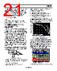
21 / 25 page  Data Sheet ADP5600 Rev. 0 | Page 21 of 25 For the best noise performance, choose the LDO output voltage nearest to the desired adjustable LDO output voltage without exceeding it. For example, if the desired adjustable LDO output voltage is −3.3 V, then choose the −2.5 V LDO output voltage (SEL1 = GND, SEL2 = floating), and place a resistor divider between LDO_OUT, FB, and ground. The programmed adjustable output voltage, VADJ, can be calculated as 1 ADJ LDO_OUT R1 VV R2 where: VADJ is the programmed adjustable LDO output voltage. VLDO_OUT is the LDO output voltage when the LDO_OUT pin is shorted to the FB pin. R1 is the feedback resistor between LDO_OUT and FB. R2 is the feedback resistor between FB and GND (R2 is recommended to be 40 kΩ or higher). NOISE REDUCTION The low output noise of the ADP5600 is achieved by keeping the LDO error amplifier in unity gain and setting the reference voltage equal to the output voltage. The ADP5600 uses two feed- back resistors to adjust the output of the LDO. The disadvantage of this LDO scheme is that the output voltage noise is proportional to the error amplifier gain and total feedback resistance. The LDO circuit can be modified slightly to reduce the output voltage noise to levels close to that of the fixed output of the ADP5600. The circuit shown in Figure 59 adds two additional components to the output voltage setting resistor divider. CNR and RNR are added in parallel with R2 to reduce the ac gain of the error amplifier. RNR is chosen to be nearly equal to R2, limiting the ac gain of the error amplifier to approximately 6 dB. The actual gain is the parallel combination of RNR and R1 divided by R2. This resistance ensures that the error amplifier always operates at greater than unity gain. CNR is chosen by setting the reactance of CNR equal to R1 − RNR at a frequency between 10 Hz and 100 Hz. This capacitance sets the frequency where the ac gain of the error amplifier is 3 dB down from its dc gain. Figure 59. Noise Reduction Modification The noise of the adjustable LDO is found by using the following formula, assuming the noise of a fixed output LDO is approxi- mately 59 μV: Noise = 59 μV × (RPAR + R2) ÷ R2 where RPAR is a parallel combination of R1 and RNR. Based on the component values shown in Figure 59, the ADP5600 has the following characteristics: • DC gain of 3 (9.54 dB) • High frequency ac gain of 1.67 (4.44 dB) • Measured rms noise of the adjustable LDO at −100 mA without noise reduction of ~163 μV rms • Measured rms noise of the adjustable LDO at −100 mA with noise reduction circuit of ~99 μV rms Figure 60 shows the difference in noise spectral density for the adjustable ADP5600 set to −7.5 V with and without the noise reduction network. In the 20 Hz to 20 kHz frequency range, the reduction in noise is observable. Figure 60. VADJ = −7.5 V Adjustable ADP5600 With and Without the Noise Reduction Network (CNR and RNR) CHANGING THE OSCILLATOR SOURCE ON-THE-FLY The Synchronization section describes how the charge pumps react on application and removal of an external clock on the SYNC pin. The charge pump frequency transitions smoothly upon syncing to the external clock. However, upon removal of the external clock, the charge pump stops switching, which causes a drop at CPOUT, leaving the CCPOUT supplying the charge requirement of the output (see Figure 61). Figure 61. Response of CPOUT upon Removal of the External Clock on SYNC GND LDO_OUT CLDO_OUT 2.2µF R2 75kΩ RNR 75kΩ CNR 100nF VADJ = –7.5V R1 150kΩ FB + + 10,000 FREQUENCY (Hz) 1,000 100 10 10 100 1k 10k 100k 1M 10M 1 0.1 WITHOUT NOISE REDUCTION WITH NOISE REDUCTION CH1 5.00V BW CH2 5.00V BW CH3 5.00V BW CH4 5.00V BW M40µs A CH2 TIMEOUT 2 3 4 T C1+ SYNC VCPOUT VIN 190.65µs –2.1V 530kHz 1.1MHz 2.2MHz |
|
|
ссылки URL |
| Вашему бизинису помогли Аллдатащит? [ DONATE ] |
Что такое Аллдатащит | реклама | контакт | Конфиденциальность | Ссылка на техническое описание | обмен ссыками | поиск по производителю All Rights Reserved©Alldatasheet.com |
| Russian : Alldatasheetru.com | Korean : Alldatasheet.co.kr | Spanish : Alldatasheet.es | French : Alldatasheet.fr | Italian : Alldatasheetit.com Portuguese : Alldatasheetpt.com | Polish : Alldatasheet.pl | Vietnamese : Alldatasheet.vn Indian : Alldatasheet.in | Mexican : Alldatasheet.com.mx | British : Alldatasheet.co.uk | New Zealand : Alldatasheet.co.nz |
|
Family Site : ic2ic.com |
icmetro.com |
 Russian ▼
 English
 Chinese
 German
 Japanese
 Russian
 Korean
 Spanish
 French
 Italian
 Portuguese
 Polish
 Vietnamese
 Indian
 Mexican
 British
 New Zealand