|
поискавой системы для электроныых деталей |
|
|
поискавой системы для электроныых деталей |
|
ADP5600ACPZ-R7 датащи(PDF) 15 Page - Analog Devices |
|
|
|||||||||||||||||||||||||||||
ADP5600ACPZ-R7 датащи(HTML) 15 Page - Analog Devices |
|
|
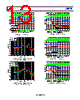
15 / 25 page  Data Sheet ADP5600 Rev. 0 | Page 15 of 26 In Figure 41, an oscillator generating antiphase signals (φ1 and φ2) controls the S1, S2, and S3, S4 switches. During the charging phase, φ1, the S1 and S2 switches are closed, charging CFLY up to the voltage at VIN. During output phase, φ2, S1 and S2 open and S3 and S4 close. The positive terminal of CFLY is connected to GND via S3 and the negative terminal of CFLY connects to OUT via S4. The charge on CFLY is transferred to COUT during φ2. The net result at steady state is voltage inversion at OUT with respect to GND. Ideally, capacitor COUT maintains its voltage during φ1. However, due to limited storage capacity, this voltage drops due to the load (IOUT) until φ2 arrives. This discharging and charging action of COUT is the output ripple. The charge transfer efficiency depends on the on-resistance of the switches, the frequency at which they are being switched, and on the equivalent series resistance (ESR) of the external capacitors. For minimum losses and maximum efficiency, capacitors with low ESR are, therefore, recommended. The charging and discharging current are always discontinuous and the output voltage ripple for the charge pumps is always 2 OUT OUT OSC OUT I V fC Similarly, the input voltage ripple is always 2 OUT IN OSC IN I V fC where: ΔVOUT is the output voltage ripple. ΔVIN is the input voltage ripple. IOUT is the charge pump load current. fOSC is the charge pump switching frequency. CIN is the charge pump input capacitor. COUT is the charge pump output capacitor. Therefore, the voltage ripple (noise) can only be improved by decreasing IOUT (impractical), increasing the switching frequency (less efficient), or increasing the capacitance (costly). By adding another charge pump of the opposite phase, the ADP5600 offers a solution with an almost continuous current flowing at the input and output nodes, greatly reducing the voltage ripple. INTERLEAVED INVERTING CHARGE PUMP OPERATION The ADP5600 has two inverting charge pumps that operate in an interleaving manner, requiring the use of two small flying capacitors (CC1 and CC2), which are typically of the same value. Each fly capacitor operates on a separate charge pump inverter that runs out of phase with each other. The output is then combined at CPOUT as shown in Figure 42. The interleaving operation results in a periodic ripple that is twice the frequency of the oscillator. Figure 42. Interleaved Operation This approach provides a roughly constant input and output current that dramatically reduces the voltage ripple. For an interleaved inverting charge pump, the output voltage ripple is given by 2 4 1 CPOUT CPOUT CPOUT OUT ON OSC CPOUT C1 CPOUT I VI R R fC C C where: ΔVCPOUT is the ripple voltage in CPOUT. ICPOUT is the load current in CPOUT. fOSC is the charge pump switching frequency. CCPOUT is the output capacitor in CPOUT. CC1 is the fly capacitor. ROUT is the effective output resistance of the charge pump. RON is the average on resistance of the four switches. β = 8 1 OSC ON C1 ef R C . A comparison of the conventional charge pump topology and the interleaving approach is shown in Figure 43 and Figure 44. Figure 43. Noninterleaved Charge Pump Operation (fOSC = 500 kHz, CIN = 10 μF, C1 = 1 μF, C2 = Float, CCPOUT = 10 μF) + CCPOUT CPOUT = –VIN VIN C2+ C2– OSCILLATOR Ф1 Ф2 + CC2 VIN + CIN CPH1 CPH2 CPG1 CPG2 FNG1 FNG2 FNO1 FNO2 C1+ C1– + CC1 CH1 2.00mVΩBW CH2 2.00mVΩBW CH3 10V BW M1.00µs A CH4 6.80V 1 2 3 T VIN C+ CPOUT T 0s |
|
|
ссылки URL |
| Вашему бизинису помогли Аллдатащит? [ DONATE ] |
Что такое Аллдатащит | реклама | контакт | Конфиденциальность | Ссылка на техническое описание | обмен ссыками | поиск по производителю All Rights Reserved©Alldatasheet.com |
| Russian : Alldatasheetru.com | Korean : Alldatasheet.co.kr | Spanish : Alldatasheet.es | French : Alldatasheet.fr | Italian : Alldatasheetit.com Portuguese : Alldatasheetpt.com | Polish : Alldatasheet.pl | Vietnamese : Alldatasheet.vn Indian : Alldatasheet.in | Mexican : Alldatasheet.com.mx | British : Alldatasheet.co.uk | New Zealand : Alldatasheet.co.nz |
|
Family Site : ic2ic.com |
icmetro.com |
 Russian ▼
 English
 Chinese
 German
 Japanese
 Russian
 Korean
 Spanish
 French
 Italian
 Portuguese
 Polish
 Vietnamese
 Indian
 Mexican
 British
 New Zealand