|
поискавой системы для электроныых деталей |
|
|
поискавой системы для электроныых деталей |
|
ADP5600ACPZ-R7 датащи(PDF) 16 Page - Analog Devices |
|
|
|||||||||||||||||||||||||||||
ADP5600ACPZ-R7 датащи(HTML) 16 Page - Analog Devices |
|
|
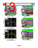
16 / 25 page  ADP5600 Data Sheet Rev. 0 | Page 16 of 25 Figure 44. Interleaved Charge Pump Operation (fOSC = 500 kHz, CIN = 10 μF, C1 = C2 = 1 μF, CCPOUT = 10 μF) CHARGE PUMP OUTPUT RESISTANCE The output resistance is the main loss contributor in a charge pump switching converter. A simplified model is shown in Figure 45 where the output resistance is just before the output capacitor. The model shows that when a load current, ICPOUT, is pulled from VCPOUT, a resulting voltage drop is generated. Figure 45. Simplified Output Resistance Model Always consider the output resistance when designing for a desired output voltage because the voltage drop across the charge pump scales with the load current. To estimate ADP5600 output resistance, ROUT, use the following equation: ROUT = 1/(2 × C1 × fOSC) + 4 × RON + 2 × RC1_ESR where: RON is the average on resistance of the four switches, the typical value is ~2.1 Ω. RC1_ESR is the ESR of C1. NEGATIVE LDO REGULATOR Internally, the ADP5600 has a negative LDO regulator that consists of a reference, an error amplifier, a feedback voltage divider, and an N-channel metal-oxide-semiconductor (NMOS) pass transistor. Current flows from CPOUT to LDO_OUT via the NMOS pass transistor, which is controlled by the error amplifier. The error amplifier compares the reference voltage with the feed- back voltage from the output and amplifies the difference. If the feedback voltage is more positive than the reference voltage, the gate of the NMOS transistor is pulled toward GND, allowing more current to pass and increasing the output voltage magnitude. If the feedback voltage is more negative than the reference voltage, the gate of the NMOS transistor is pulled toward VCPOUT, allowing less current to pass and decreasing the output voltage. Figure 46. Simplified LDO Model STARTUP AND SOFT START Charge Pump Startup The ADP5600 starts switching when VIN ≥ UVLORISING and VEN ≥ ENTH. If left unprotected, large inrush currents can flow from CIN to C1 and C2 until the capacitors reach their steady state values. Therefore, the ADP5600 implements a controlled soft start profile where the maximum input current is limited to 200 mA over a time period. If VIN ≥ UVLORISING and VEN < ENTH, the output pull-down resistor is enabled, discharging the output. If VIN < UVLORISING, the output pull-down resistor is disabled. LDO Soft Start If the voltage magnitude at CPOUT exceeds PGTH_CP, the LDO is enabled and starts to ramp up the reference voltage at the input of the error amplifier, causing a soft start response at LDO_OUT. Estimate the LDO soft start time, tSS, using the following formula: tSS = (CSS × VLDO_OUT)/ISS where: VLDO_OUT, output voltage according to SEL1 and SEL2. CSS, internal soft start capacitor, is 98.4 pF. ISS, internal source current to CSS, is 1 μA. If VCPOUT is less negative than PGTH_CP, the LDO is disabled and the output pull-down resistor is enabled. Figure 47 shows the start-up response of ADP5600 at different LDO output voltages. Figure 47. Start-Up Response at Various LDO Output Voltages CH1 2.00mVΩBW CH2 2.00mVΩBW CH3 10V BW M1.00µs A CH4 6.80V 1 2 3 T 0s T VIN C+ CPOUT CCPOUT ICPOUT ROUT VCPOUT –VIN + CPOUT SEL1 SEL2 PGOOD LDO_OUT FB GND + – VREF ×1 + – PGTH REFERENCE GENERATOR + – PGTH_CP 10 –10 –4 –6 –8 4 0 8 2 –2 6 –4 4 –1 3 –2 1 2 0 –3 TIME (ms) VIN VEN VCPOUT VLDO_OUT4 = –5.0V VLDO_OUT3 = –2.5V VLDO_OUT2 = –1.5V VLDO_OUT1 = –0.505V |
|
|
ссылки URL |
| Вашему бизинису помогли Аллдатащит? [ DONATE ] |
Что такое Аллдатащит | реклама | контакт | Конфиденциальность | Ссылка на техническое описание | обмен ссыками | поиск по производителю All Rights Reserved©Alldatasheet.com |
| Russian : Alldatasheetru.com | Korean : Alldatasheet.co.kr | Spanish : Alldatasheet.es | French : Alldatasheet.fr | Italian : Alldatasheetit.com Portuguese : Alldatasheetpt.com | Polish : Alldatasheet.pl | Vietnamese : Alldatasheet.vn Indian : Alldatasheet.in | Mexican : Alldatasheet.com.mx | British : Alldatasheet.co.uk | New Zealand : Alldatasheet.co.nz |
|
Family Site : ic2ic.com |
icmetro.com |
 Russian ▼
 English
 Chinese
 German
 Japanese
 Russian
 Korean
 Spanish
 French
 Italian
 Portuguese
 Polish
 Vietnamese
 Indian
 Mexican
 British
 New Zealand