|
поискавой системы для электроныых деталей |
|
|
поискавой системы для электроныых деталей |
|
MCP631 датащи(PDF) 25 Page - Microchip Technology |
|
|
|||||||||||||||||||||||||||||
MCP631 датащи(HTML) 25 Page - Microchip Technology |
|
|
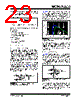
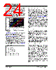
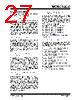
25 / 42 page  © 2009 Microchip Technology Inc. DS22197A-page 25 MCP631/2/3/5 Sometimes, it helps to place guard traces next to victim traces. They should be on both sides of the victim trace, and as close as possible. Connect guard traces to ground plane at both ends, and in the middle for long traces. Use coax cables, or low inductance wiring, to route signal and power to and from the PCB. Mutual and self inductance of power wires is often a cause of crosstalk and unusual behavior. 4.7 Typical Applications 4.7.1 POWER DRIVER WITH HIGH GAIN Figure 4-10 shows a power driver with high gain (1 + R2/R1). The MCP631/2/3/5 op amp’s short circuit current makes it possible to drive significant loads. The calibrated input offset voltage supports accurate response at high gains. R3 should be small, and equal to R1||R2, in order to minimize the bias current induced offset. FIGURE 4-10: Power Driver. 4.7.2 OPTICAL DETECTOR AMPLIFIER Figure 4-11 shows a transimpedance amplifier, using the MCP63X op amp, in a photo detector circuit. The photo detector is a capacitive current source. RF provides enough gain to produce 10 mV at VOUT. CF stabilizes the gain and limits the transimpedance bandwidth to about 1.1 MHz. RF’s parasitic capacitance (e.g., 0.2 pF for a 0805 SMD) acts in parallel with CF. FIGURE 4-11: Transimpedance Amplifier for an Optical Detector. 4.7.3 H-BRIDGE DRIVER Figure 4-12 shows the MCP632 dual op amp used as a H-bridge driver. The load could be a speaker or a DC motor. FIGURE 4-12: H-Bridge Driver. This circuit automatically makes the noise gains (GN) equal, when the gains are set properly, so that the frequency responses match well (in magnitude and in phase). Equation 4-7 shows how to calculate RGT and RGB so that both op amps have the same DC gains; GDM needs to be selected first. EQUATION 4-7: Equation 4-8 gives the resulting common mode and differential mode output voltages. EQUATION 4-8: R1 R2 VIN VDD/2 VOUT R3 RL MCP63X Photo Detector CD CF RF VDD/2 30pF 100 k Ω 1.5 pF ID 100 nA VOUT MCP63X RF RF VIN VOT RF RGB VOB VDD/2 RGT RL ½ MCP632 ½ MCP632 G DM V OT V OB – V IN V DD 2 ⁄ – -------------------------------- 1 V/V ≥ ≡ R GT R F G DM 2 ⁄ () 1 – --------------------------------- = R GB R F G DM 2 ⁄ ------------------- = V OT V + OB 2 --------------------------- V DD 2 ----------- = V OT V – OB G DM VIN V DD 2 ----------- – ⎝⎠ ⎛⎞ = |
|
ссылки URL |
| Вашему бизинису помогли Аллдатащит? [ DONATE ] |
Что такое Аллдатащит | реклама | контакт | Конфиденциальность | Ссылка на техническое описание | обмен ссыками | поиск по производителю All Rights Reserved©Alldatasheet.com |
| Russian : Alldatasheetru.com | Korean : Alldatasheet.co.kr | Spanish : Alldatasheet.es | French : Alldatasheet.fr | Italian : Alldatasheetit.com Portuguese : Alldatasheetpt.com | Polish : Alldatasheet.pl | Vietnamese : Alldatasheet.vn Indian : Alldatasheet.in | Mexican : Alldatasheet.com.mx | British : Alldatasheet.co.uk | New Zealand : Alldatasheet.co.nz |
|
Family Site : ic2ic.com |
icmetro.com |
 Russian ▼
 English
 Chinese
 German
 Japanese
 Russian
 Korean
 Spanish
 French
 Italian
 Portuguese
 Polish
 Vietnamese
 Indian
 Mexican
 British
 New Zealand