|
поискавой системы для электроныых деталей |
|
|
поискавой системы для электроныых деталей |
|
MCP631 датащи(PDF) 23 Page - Microchip Technology |
|
|
|||||||||||||||||||||||||||||
MCP631 датащи(HTML) 23 Page - Microchip Technology |
|
|
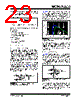
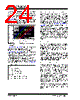
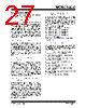
23 / 42 page  © 2009 Microchip Technology Inc. DS22197A-page 23 MCP631/2/3/5 The power de-rating across temperature for an op amp in a particular package can be easily calculated (assuming equal power dissipations): EQUATION 4-5: Several techniques are available to reduce ΔTJA for a given POAmax: • Lower θJA - Use another package - PCB layout (ground plane, etc.) - Heat sinks and air flow • Reduce POAmax - Increase RL - Limit IOUT (using RSER) - Decrease VDD 4.3 Improving Stability 4.3.1 CAPACITIVE LOADS Driving large capacitive loads can cause stability problems for voltage feedback op amps. As the load capacitance increases, the feedback loop’s phase margin decreases and the closed-loop bandwidth is reduced. This produces gain peaking in the frequency response, with overshoot and ringing in the step response. A unity gain buffer (G = +1) is the most sensitive to capacitive loads, though all gains show the same general behavior. When driving large capacitive loads with these op amps (e.g., > 20 pF when G = +1), a small series resistor at the output (RISO in Figure 4-6) improves the feedback loop’s phase margin (stability) by making the output load resistive at higher frequencies. The bandwidth will be generally lower than the bandwidth with no capacitive load. FIGURE 4-6: Output Resistor, RISO stabilizes large capacitive loads. Figure 4-7 gives recommended RISO values for different capacitive loads and gains. The x-axis is the normalized load capacitance (CL/GN), where GN is the circuit’s noise gain. For non-inverting gains, GN and the Signal Gain are equal. For inverting gains, GN is 1+|Signal Gain| (e.g., -1 V/V gives GN =+2 V/V). FIGURE 4-7: Recommended RISO Values for Capacitive Loads. After selecting RISO for your circuit, double check the resulting frequency response peaking and step response overshoot. Modify RISO’s value until the response is reasonable. Bench evaluation and simulations with the MCP631/2/3/5 SPICE macro model are helpful. 4.3.2 GAIN PEAKING Figure 4-8 shows an op amp circuit that represents non-inverting amplifiers (VM is a DC voltage and VP is the input) or inverting amplifiers (VP is a DC voltage and VM is the input). The capacitances CN and CG represent the total capacitance at the input pins; they include the op amp’s common mode input capacitance (CCM), board parasitic capacitance and any capacitor placed in parallel. FIGURE 4-8: Amplifier with Parasitic Capacitance. CG acts in parallel with RG (except for a gain of +1 V/V), which causes an increase in gain at high frequencies. CG also reduces the phase margin of the feedback loop, which becomes less stable. This effect can be reduced by either reducing CG or RF. n θ JA TJmax –TA POAmax ≤ Where: TJmax = absolute maximum junction temperature RISO VOUT CL RG RF RN MCP63X 10 100 1,000 1.E-12 1.E-11 1.E-10 1.E-09 1.E-08 Normalized Capacitance; CL/GN (F) GN = +1 GN ≥ +2 10p 100p 1n 10n VP RF VOUT RN CN VM RG CG MCP63X |
|
ссылки URL |
| Вашему бизинису помогли Аллдатащит? [ DONATE ] |
Что такое Аллдатащит | реклама | контакт | Конфиденциальность | Ссылка на техническое описание | обмен ссыками | поиск по производителю All Rights Reserved©Alldatasheet.com |
| Russian : Alldatasheetru.com | Korean : Alldatasheet.co.kr | Spanish : Alldatasheet.es | French : Alldatasheet.fr | Italian : Alldatasheetit.com Portuguese : Alldatasheetpt.com | Polish : Alldatasheet.pl | Vietnamese : Alldatasheet.vn Indian : Alldatasheet.in | Mexican : Alldatasheet.com.mx | British : Alldatasheet.co.uk | New Zealand : Alldatasheet.co.nz |
|
Family Site : ic2ic.com |
icmetro.com |
 Russian ▼
 English
 Chinese
 German
 Japanese
 Russian
 Korean
 Spanish
 French
 Italian
 Portuguese
 Polish
 Vietnamese
 Indian
 Mexican
 British
 New Zealand