|
поискавой системы для электроныых деталей |
|
|
поискавой системы для электроныых деталей |
|
RA4M2 датащи(PDF) 27 Page - Renesas Technology Corp |
|
|
|||||||||||||||||||||||||||||
RA4M2 датащи(HTML) 27 Page - Renesas Technology Corp |
|
|
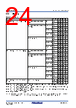
27 / 93 page  Table 2.7 Operating and standby current (2 of 2) Parameter Symbol Min Typ Max Unit Test conditions Analog power supply current During 12-bit A/D conversion AICC — 0.8 1.1 mA — Temperature sensor — 0.1 0.2 mA — During D/A conversion (per unit) Without AMP output — 0.1 0.2 mA — With AMP output — 0.6 1.1 mA — Waiting for A/D, D/A conversion (all units) — 0.5 1.0 mA — ADC12, DAC12 in standby modes (all units)*9 — 0.4 4.0 µA — Reference power supply current (VREFH0) During 12-bit A/D conversion (unit 0) AIREFH0 — 70 120 µA — Waiting for 12-bit A/D conversion (unit 0) — 0.07 0.5 µA — ADC12 in standby modes (unit 0) — 0.07 0.5 µA — Reference power supply current (VREFH) During D/A conversion (per unit) Without AMP output AIREFH — 0.1 0.4 mA — With AMP ouput — 0.1 0.4 mA — Waiting for D/A (all units) conversion — 0.07 0.8 µA — USB operating current Low speed USB ICCUSBLS — 3.5 6.5 mA VCC_USB Full speed USB ICCUSBFS — 4.0 10.0 mA VCC_USB LDO operating current (1 unit)*15 ICCLDO — 0.18 — mA — PLL2-LDO operating current ICCPLL2LDO — 0.21 — mA — Note 1. Supply current values are with all output pins unloaded and all input pull-up MOSs in the off state. Note 2. Measured with clocks supplied to the peripheral functions. This does not include the BGO operation. Note 3. ICC depends on f (ICLK) as follows. ICC Max. = 0.53 × f + 12 (max. operation in high-speed mode) ICC Typ. = 0.05 × f + 1.85 (normal operation in high-speed mode, all peripheral clocks disabled) ICC Typ. = 0.12 × f + 0.69 (low-speed mode) ICC Max. = 0.13 × f + 12 (sleep mode) Note 4. This does not include the BGO operation. Note 5. Supply of the clock signal to peripherals is stopped in this state. This does not include the BGO operation. Note 6. FCLK, PCLKA, PCLKB, PCLKC, and PCLKD are set to divided by 64 (1.563 MHz). Note 7. FCLK, PCLKA, PCLKB, PCLKC, and PCLKD are set to divided by 64 (3.125 MHz). Note 8. Reference value Note 9. When the MCU is in Software Standby mode or the MSTPCRD.MSTPD16 (12-Bit A/D Converter 0 Module Stop bit) and MSTPCRD.MSTPD20 (12-bit D/A converter module stop bit) are in the module-stop state. Note 10. FCLK, PCLKA, PCLKB, PCLKC, and PCLKD are set to divided by 64 (15.6 kHz). Note 11. PCLKA, PCLKB, PCLKC, and PCLKD are set to divided by 64 (512 Hz). FCLK is the same frequency as that of ICLK. Note 12. PLL output frequency = 100MHz. Note 13. PLL output frequency = 200MHz. Note 14. PLL2-LDO disabled. Note 15. n = 0, 1 RA4M2 Datasheet 2. Electrical Characteristics R01DS0367EJ0140 Rev.1.40 May 9, 2025 Page 27 of 93 |
|
ссылки URL |
| Вашему бизинису помогли Аллдатащит? [ DONATE ] |
Что такое Аллдатащит | реклама | контакт | Конфиденциальность | Ссылка на техническое описание | обмен ссыками | поиск по производителю All Rights Reserved©Alldatasheet.com |
| Russian : Alldatasheetru.com | Korean : Alldatasheet.co.kr | Spanish : Alldatasheet.es | French : Alldatasheet.fr | Italian : Alldatasheetit.com Portuguese : Alldatasheetpt.com | Polish : Alldatasheet.pl | Vietnamese : Alldatasheet.vn Indian : Alldatasheet.in | Mexican : Alldatasheet.com.mx | British : Alldatasheet.co.uk | New Zealand : Alldatasheet.co.nz |
|
Family Site : ic2ic.com |
icmetro.com |
 Russian ▼
 English
 Chinese
 German
 Japanese
 Russian
 Korean
 Spanish
 French
 Italian
 Portuguese
 Polish
 Vietnamese
 Indian
 Mexican
 British
 New Zealand