|
поискавой системы для электроныых деталей |
|
|
поискавой системы для электроныых деталей |
|
LTC3404MPMS8 датащи(PDF) 13 Page - Linear Technology |
|
|
|||||||||||||||||||||||||||||
LTC3404MPMS8 датащи(HTML) 13 Page - Linear Technology |
|
|
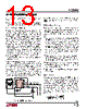
13 / 16 page  13 LTC3404 3404fb APPLICATIO S I FOR ATIO Figure 7. LTC3404 Layout Diagram – + RUN ITH VFB GND PLL LPF SYNC/MODE SW LTC3404 CC2 CC1 RC COUT 3404 F07 L1 VIN BOLD LINES INDICATE HIGH CURRENT PATHS 1 2 3 4 8 7 6 5 OPTIONAL + – + VOUT VIN R2 CIN + R1 which is below the maximum junction temperature of 125 °C. Note that at higher supply voltages, the junction tempera- ture is lower due to reduced switch resistance (RDS(ON)). Checking Transient Response The regulator loop response can be checked by looking at the load transient response. Switching regulators take several cycles to respond to a step in load current. When a load step occurs, VOUT immediately shifts by an amount equal to ( ΔILOAD • ESR), where ESR is the effective series resistance of COUT. ΔILOAD also begins to charge or discharge COUT, which generates a feedback error signal. The regulator loop then acts to return VOUT to its steady- state value. During this recovery time VOUT can be moni- tored for overshoot or ringing that would indicate a stabil- ity problem. The internal compensation provides adequate compensation for most applications. But if additional compensation is required, the ITH pin can be used for external compensation using RC, CC1 as shown in Figure 7. (The 47pF capacitor, CC2, is typically needed for noise decoupling.) A second, more severe transient is caused by switching in loads with large (>1 μF) supply bypass capacitors. The discharged bypass capacitors are effectively put in parallel with COUT, causing a rapid drop in VOUT. No regulator can deliver enough current to prevent this problem if the load switch resistance is low and it is driven quickly. The only solution is to limit the rise time of the switch drive so that the load rise time is limited to approximately (25 • CLOAD). Thus, a 10 μF capacitor charging to 3.3V would require a 250 μs rise time, limiting the charging current to about 130mA. PC Board Layout Checklist When laying out the printed circuit board, the following checklist should be used to ensure proper operation of the LTC3404. These items are also illustrated graphically in the layout diagram of Figure 7. Check the following in your layout: 1. Are the signal and power grounds segregated? The LTC3404 signal ground consists of the resistive divider, the optional compensation network (RC and CC1) and CC2. The power ground consists of the (–) plate of CIN, the (–) plate of COUT and Pin 4 of the LTC3404. The power ground traces should be kept short, direct and wide. The signal ground and power ground should converge to a common node in a star- ground configuration. 2. Does the VFB pin connect directly to the feedback resistors? The resistive divider R1/R2 must be con- nected between the (+) plate of COUT and signal ground. 3. Does the (+) plate of CIN connect to VIN as closely as possible? This capacitor provides the AC current to the internal power MOSFETs. 4. Keep the switching node SW away from sensitive small signal nodes. Design Example As a design example, assume the LTC3404 is used in a single lithium-ion battery-powered cellular phone applica- tion. The input voltage will be operating from a maximum of 4.2V down to about 2.7V. The load current requirement is a maximum of 0.3A but most of the time it will be in standby mode, requiring only 2mA. Efficiency at both low and high load currents is important. Output voltage is 2.5V. With this information we can calculate L using equation (1), L fI V V V L OUT OUT IN = () Δ() − ⎛ ⎝⎜ ⎞ ⎠⎟ 1 1 (3) |
|
|
ссылки URL |
| Вашему бизинису помогли Аллдатащит? [ DONATE ] |
Что такое Аллдатащит | реклама | контакт | Конфиденциальность | Ссылка на техническое описание | обмен ссыками | поиск по производителю All Rights Reserved©Alldatasheet.com |
| Russian : Alldatasheetru.com | Korean : Alldatasheet.co.kr | Spanish : Alldatasheet.es | French : Alldatasheet.fr | Italian : Alldatasheetit.com Portuguese : Alldatasheetpt.com | Polish : Alldatasheet.pl | Vietnamese : Alldatasheet.vn Indian : Alldatasheet.in | Mexican : Alldatasheet.com.mx | British : Alldatasheet.co.uk | New Zealand : Alldatasheet.co.nz |
|
Family Site : ic2ic.com |
icmetro.com |
 Russian ▼
 English
 Chinese
 German
 Japanese
 Russian
 Korean
 Spanish
 French
 Italian
 Portuguese
 Polish
 Vietnamese
 Indian
 Mexican
 British
 New Zealand